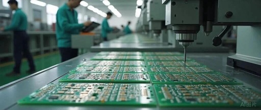
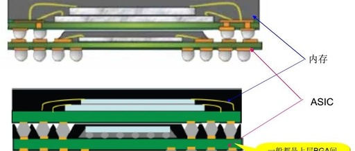
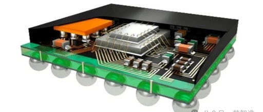
Comprehensive Solutions for PCB Deformation in BGA Reflow Soldering

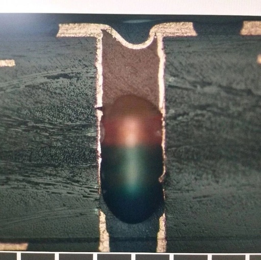
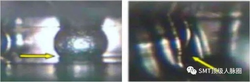
📌 Problem Overview BGA components are prone to deformation during the reflow soldering process due to high thermal stress. This deformation can lead to poor contact between BGA solder balls and pads, resulting in cold solder joints, short circuits, or solder joint fractures due to stress concentration in later usage. The following table summarizes the … Read more