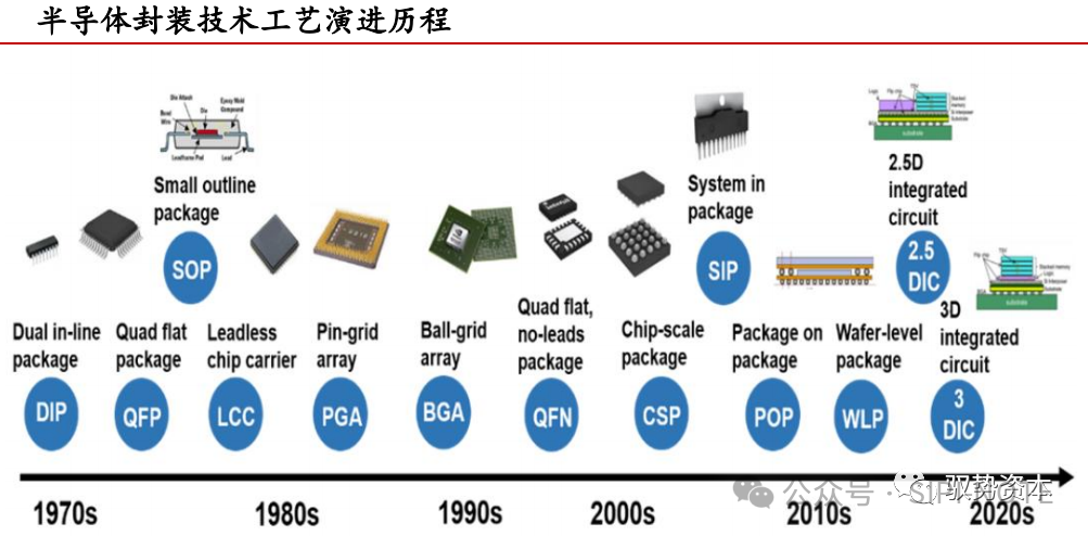
The development of packaging has evolved from the early DIP to the current 3D ICs [1][2], with a variety of packaging types emerging. Just the QF series has spawned a long list of types such as QFN (no leads), QFP (with leads)… There are many choices in terms of product applications [3], and each type of packaging has its own advantages and disadvantages, depending on the application scenario.
When I saw so many types of packaging, I felt a bit overwhelmed and thought I might not be suited for the semiconductor industry. However, after getting involved, I realized that no matter how packaging changes, it ultimately needs to connect to the circuit board (PCB). There are only two common types of packaging bases, Leadframe and BGA (Ball Grid Array). The common connection methods for the chip’s IO pins are bond wire and flip chip.
Chip Connection Technologies
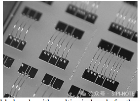
To understand packaging, we must first discuss bare chips (Die). Chip connections mainly consist of Wire Bond and Flip Chip connection technologies.
Wire Bond
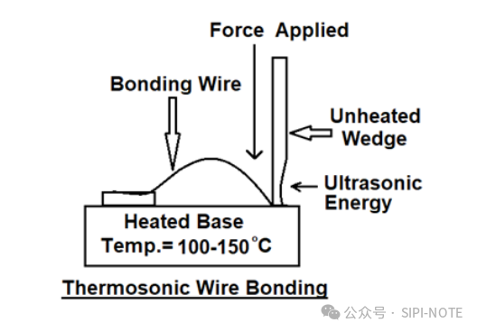
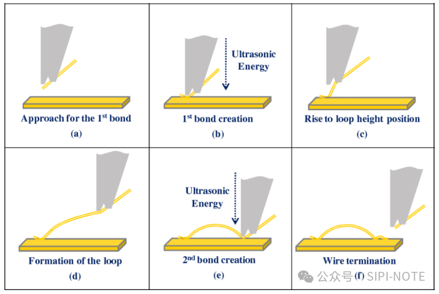
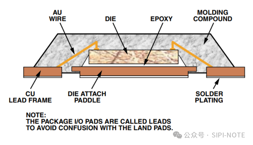
Wire Bond is a technique that connects the bond pad on the bare chip to the lead frame or finger pad on the substrate using fine metal wires. Currently, bonding methods include thermocompression, ultrasonic, and thermocompression ultrasonic bonding (don’t doubt it, it’s just the combination of the first two techniques XD).
Here, I will briefly explain the thermocompression ultrasonic bonding technology. This is currently the mainstream bonding technology in the industry. This technology combines ultrasonic vibration and heating mechanisms. During the ultrasonic bonding process, the elastic vibration between the metal wire and the bond pad breaks the oxide layer on the contact surface while generating heat, allowing for a strong bond to form between the two. Additionally, the heated base and wedge are synchronized to heat to about 150°C, which helps the atoms at the contact interface to diffuse, further enhancing the intermolecular forces, thereby increasing the strength and stability of the bond point. This is just a brief explanation; for those interested, you can refer to the literature [4]. The schematic is as follows:
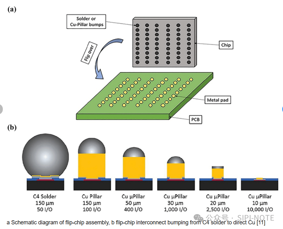
Flip Chip
Flip Chip, as the name suggests, involves flipping the bumps on the chip and directly connecting them to the substrate or PCB. As for the types of bumps, I won’t go into detail here; the common types in the industry are mainly divided into C4 Bump and Copper Pillar. In simple terms, Copper Pillar has a smaller pitch compared to C4 Bump, allowing for more I/O pads to fit on the same size die, further enhancing connection density and design flexibility.
Types of Packaging
After discussing connection methods, looking at the types of packaging becomes much clearer. They can be broadly divided into three categories: Lead frame packaging, BGA packaging, and complex structure packaging.
Lead frame packaging
Lead frame packaging can be considered the ancestor of packaging, with a relatively simple structure that has stood the test of time, supported by its low cost and durability. It has evolved from the most basic TO packaging to DIP, SO series, and QF series; detailed information can be found in ASE’s materials and literature [7][8].
BGA Packaging (Ball Grid Array)
The evolution of chip packaging to the BGA form is mainly due to the increasing number of IO pins required as chip IO counts rise. Additionally, as data rates increase, the need for lower inductance in packaging becomes critical; using lead frames poses a significant risk of failure. While the appearance of BGA types may not differ much, there are many variations, such as whether the die is fan-in or fan-out, whether a substrate or PI tape is used, and whether it is panel-level packaging or wafer-level, traditional packaging processes can lead to many different terminologies. For example, TFBGA (Thin and Fine Ball Grid Array) refers to a packaging type that is very thin with a finer ball pitch. The choice of packaging depends on the die size, IO count, and functionality.
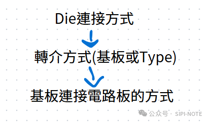
At this point, you might wonder how to remember so many packaging types. In fact, packaging can be broken down into three components: the die connection method, the intermediary substrate or type, and the connection to the circuit board. By combining these three components in different ways, we arrive at the final packaging, which is then molded.
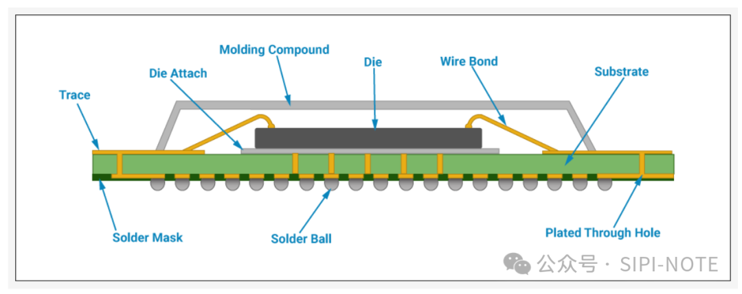
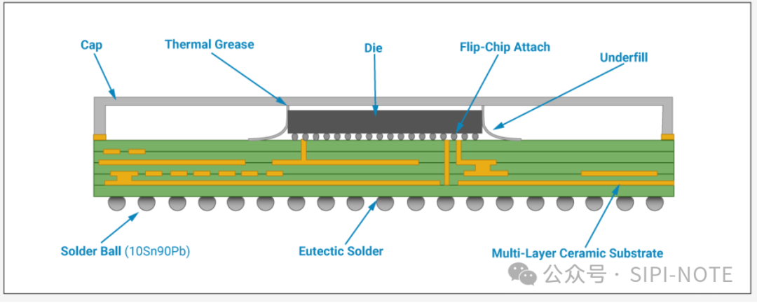
For a common packaging example, using connection methods such as bond wire and Flip Chip, the die to PCB uses a substrate, and the connection to the circuit board is through a BGA base. This results in the common Wire bond BGA and Flip chip BGA packaging types, as shown in the following images:
At this point, one might think, “Oh, it’s that simple!” But why haven’t I seen Lead frame packaging connected using Flip chip? The truth is, it doesn’t make sense to do so. Without discussing whether lead frames can be bumped, the cost alone makes it illogical; it’s a bit like using a sledgehammer to crack a nut. Here, I am simply categorizing packaging technologies; in reality, packaging is a highly specialized field, especially in terms of processes. The ability to conceptualize and execute is two different dimensions. Further exploration of complex structures will provide a better understanding; doing packaging is as challenging as working with wafers.
Complex Structure Packaging
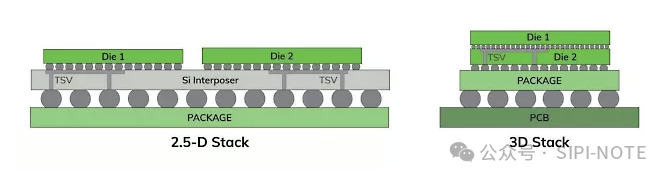
Complex structure packaging types are also numerous. It is not overly complicated; it mainly depends on how deep you want to understand (a rather vague statement 😆). The concepts are similar to those previously explained, but they include the connections between dies, packaged together. Historically, this has developed as a compromise from SOC (System on Chip) approaches, evolving into the earlier discussed SIP (System in Package). Since creating a system on a wafer is challenging (SOC), it is easier to lower the difficulty by integrating different functional dies into the same package (SIP). In earlier years, there was also MCM (Multi-Chip Module) packaging, which is somewhat similar to SIP. The evolution has led to a limit in planar designs, prompting a shift to vertical stacking (commonly referred to as 2.5D IC), and further advancements involve directly stacking dies (commonly referred to as 3D IC). These are the advanced packaging technologies that have gained attention in recent years, such as CosWoS (Chip-on-Wafer-on-Substrate) and SoIC packaging technologies, as illustrated below:
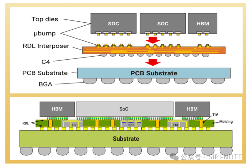
In fact, there are more advanced packaging types than CoWoS, with more mature technologies that do not use intermediary layers, instead utilizing RDL layers to expand the die’s bump area, allowing for more IO pads to connect to the substrate. [13] The above is just a conceptual overview of advanced packaging technologies. The interposer types can be broadly categorized based on material content into three architectures: Silicon interposer (currently the most mature process), RDL interposer, and Silicon bridge (EMIB). Coupled with bump types, TSVs, etc., those interested can refer to further literature.
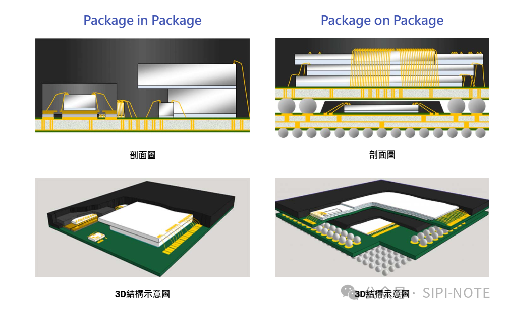
In earlier years, there were also similar technologies like PIP (Package in Package) and PoP (Package on Package), which are concepts of packaging within packaging and stacked packaging, as shown in the following image [15]:
Impact of Signal Integrity in Packaging
Finally, let’s discuss the impact of SI. A crucial factor for packaging to enhance performance is having a good packaging channel. Packaging has evolved from the early DIP to the recent CoWoS packaging, which is friendly for high-speed signal transmission. The paths have become shorter, significantly aiding in reducing both incident and reflection losses. However, SI engineers are more concerned with reflection losses in smaller packaging.
To illustrate with a literature example, in wire bond connected packaging, the most concerning structure for high-speed signal transmission paths is the bond wire structure. For high frequencies, the wire acts as a high inductance component, causing high impedance and affecting overall transmission bandwidth. This can be mitigated by adjusting the spacing between signal bond wires and ground bond wires, the size of the bond wires, and the overall structure to reduce inductance, thus achieving impedance control. The following image illustrates this (it must be noted that such structures may not be feasible for packaging manufacturers, depending on the position of the bond pad on the die 😆).
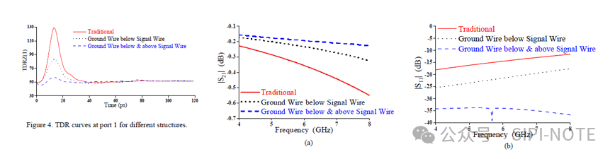
Next, regarding Wire bond BGA, to achieve good performance, reflection must be minimized. Reflection points typically include bond wire, via, and solder ball pad.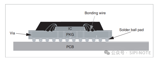
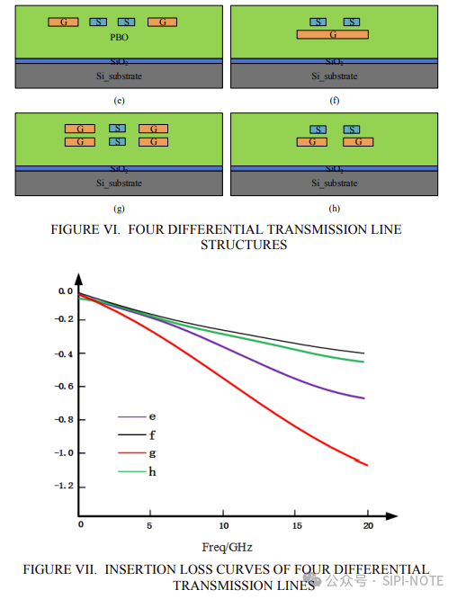
Furthermore, in advanced packaging, a more troublesome issue is the PI problem, especially with high currents, where the most intuitive IR drop issue arises. I won’t delve into that here. In SI design, it is relatively easier; the main consideration is whether there is enough routing space between signals to minimize crosstalk issues. Additionally, the small size of TSV vias must be considered to avoid excessive insertion loss due to skin effect. In RDL layers, it is unlikely to have large areas of copper laid out as reference planes for return paths. Only the so-called GND trace is present. The following image provides a simple study of the impact of different differential line routing methods on loss, as shown below [18]:
As I write this, I can’t help but feel like I’m writing a simplified review of packaging technology. For SI/PI engineers, the core of packaging design is not to pursue the most advanced packaging processes but to choose the technology that best meets product needs. In simple terms, the core consideration is still cost, which is one of the basic skills of SI/PI engineers: Trade-off! 😆