Source: Wangcai Chips
Original Author: Xiaochao Says
Why are some chips pin-packaged while mobile phone chips use bottom BGA ball grid array packaging?
The so-called chip actually only has a very small part in the middle; if you look closely at its structure, the chip is facing up, and the internal circuits connect to the surrounding bumps.
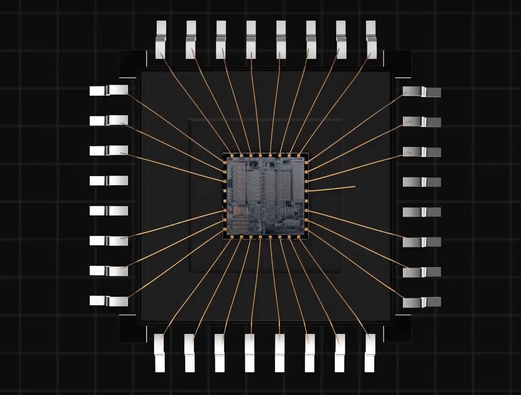
Then, one by one, gold wires thinner than a hair are bonded to the pins. After that, the casing is glued to protect it; this type of packaging is also known as wire-bond packaging.
As the functions of chips increase, the number of pins around must also increase, and correspondingly, the casing size has to be made larger. If we want to make a chip at the level of a mobile phone processor, the chip itself would need to be almost the same size as the phone, which clearly makes this type of packaging unsuitable.
Let’s take a look at how another type of packaging solves the size problem. When you open the chip casing, the chip is facing down.
Then the entire surface is covered with bumps, which are tightly attached to a wire carrier board, and the lines of the wire carrier board are directly perforated to the other side. Then, metal balls are inserted, allowing the chip to connect to the outside through these metal balls, making the area much smaller than before, and the number of pins can be significantly increased.
If the chip is used in a mobile phone, this step is still not enough. Mobile phone chips not only require core computation but also storage, baseband, and other modules, meaning that multiple chip modules need to communicate with each other and be integrated into one package. The principle is to place all chip modules facing down, with many very fine bumps.
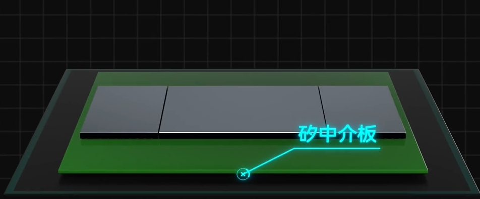
Then connect a silicon interposer, using chemical methods to create lines on the silicon interposer. These lines are also perforated, with a width of only 10 microns, about 1/10 the width of a hair. Then, metal bumps are placed at the bottom to connect to the wire carrier board. The lines of the wire carrier board are also perforated, and many metal balls are connected; this type of packaging is called 2.5D packaging. Currently, many chips use this type of packaging.
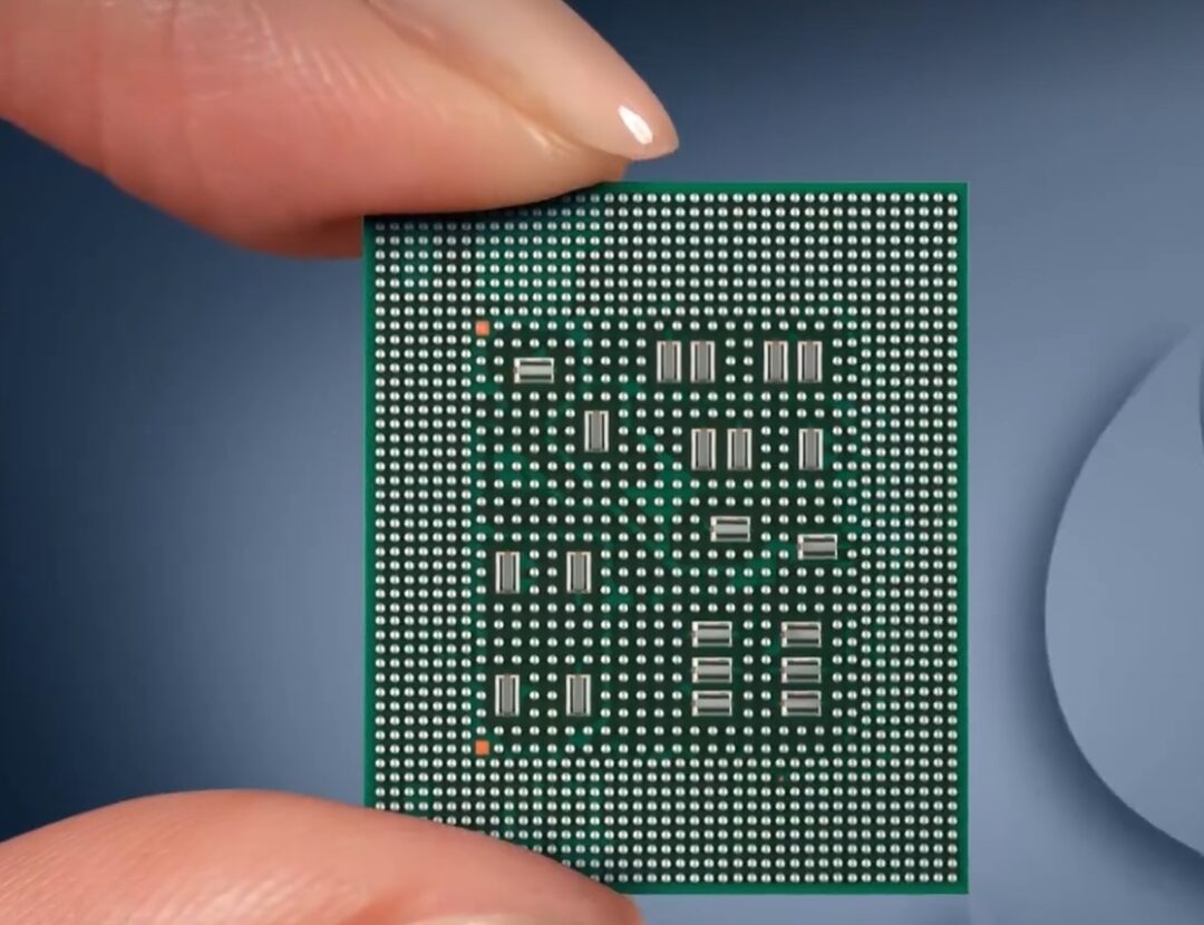
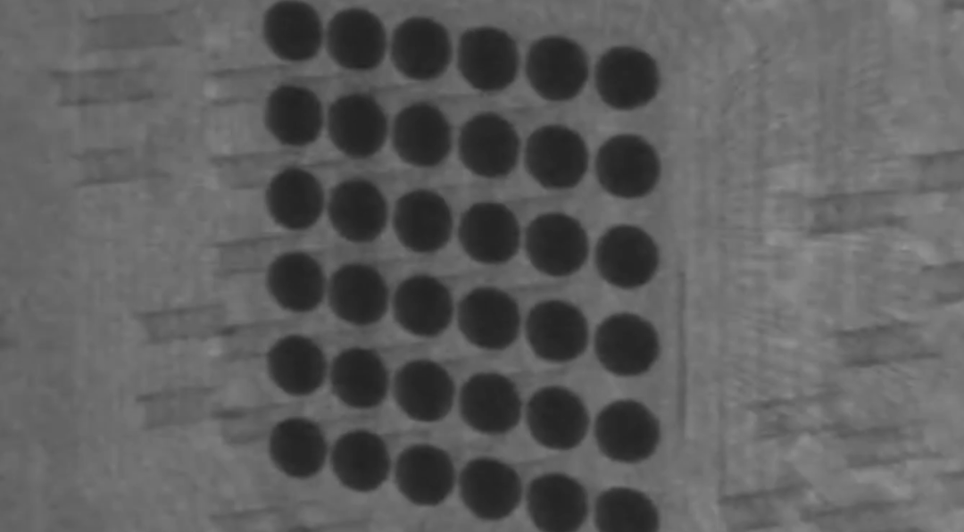
From the physical object, we can see that the metal balls on the back are very dense, and the spacing between the metal balls is also very narrow. When soldering the circuit board, if it is slightly tilted, the metal balls can easily touch the pads, so the soldering process for mobile phone chips uses SMT placement machines.
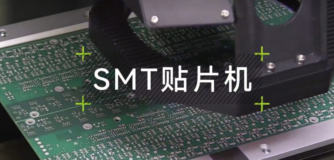
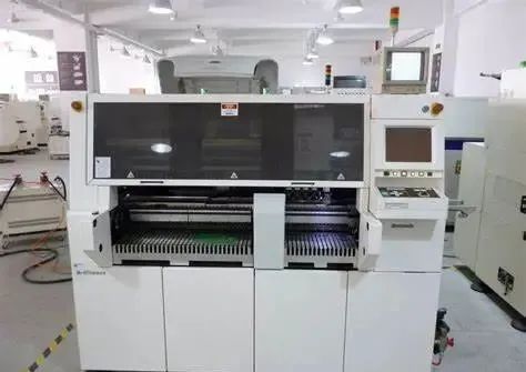
Machines are used to identify the positions of the pads for precise chip placement. To check if the pads in the middle are accurately aligned, it is impossible to see directly. Therefore, SMT factories use S-ray equipment, which works similarly to X-ray, allowing for a clear view of the internal contact conditions, and through this lens, even very fine lines can be clearly seen.
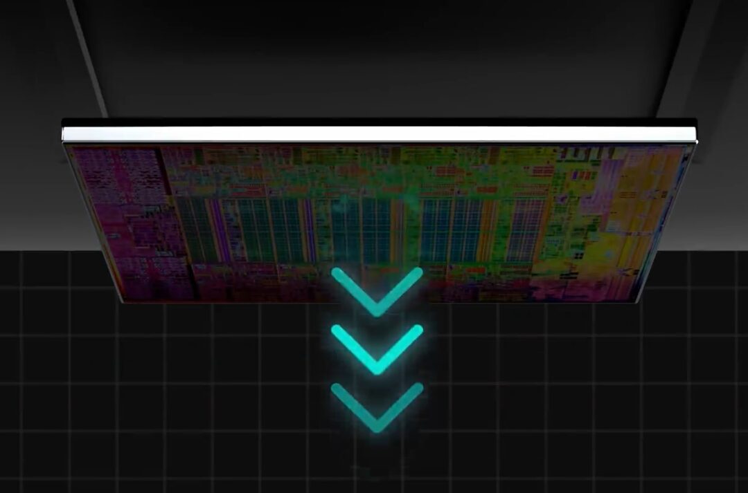
The mainstream chips currently using 2.5D packaging want to break through, regardless of how all chip modules are laid flat on one surface. However, there are even more groundbreaking technologies that involve perforating the chip itself, meaning that the middle layer of the chip maintains its original function while also having perforations for vertical connectivity. Therefore, considerations for routing and perforation must be made at the transistor level, which is extremely challenging.
Currently, the only chip capable of perforation is the DRAM memory chip. Chips that have already achieved 3D packaging are used in camera image processing chips.
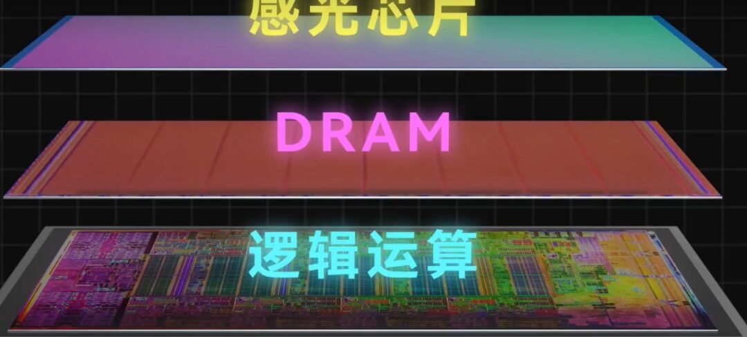
The top is used for light-sensing, the middle is DRAM for intermediate perforation, and the bottom is used for logical operations, forming a complete 3D package. Thus, the future direction for chip development is to stack all chips with perforations together, which is extremely challenging and has not yet been realized.
This concludes the principles of chip packaging.
Reprinted content only represents the author’s views
and does not represent the position of the Institute of Semiconductors, Chinese Academy of Sciences.
Editor: Qian Niao