The design differences of contact points have varying impacts on contact quality and reliability, accessibility, and subsequent solderability, which are negligible for small contact points.
1. Component Testing
As the BGA pitch and solder ball size decrease, the design of socket manufacturers faces increasing challenges to adequately test BGA packages. Socket manufacturers are focusing on various cutting-edge designs to meet the sub-millimeter pitch requirements of BGAs.
One challenge is the ability to contact all solder balls of the BGA. When connected to the printed circuit board, the solder balls melt and automatically align with the corresponding pads on the printed circuit board. Therefore, when the BGA is connected to the printed circuit board, a larger solder ball position offset is tolerable. However, during testing and aging, these variations must be tightened, as the socket contacts do not have self-alignment capabilities with the solder balls.
The design of socket probes needs to consider variations in solder ball height. The greater the difference in solder ball height, the larger the contact range required for the socket probes. At the same time, during testing, the solder balls also become more susceptible to damage. BGA aging tests are conducted at high temperatures. The combined effect of aging time and temperature will soften the solder balls, with the degree of softening depending on the solder ball material. When the test probes apply pressure, the softened solder balls may undergo severe deformation, potentially affecting contact quality during the aging process. Socket manufacturers need to ensure that the probes do not adhere to the softened solder balls and do not displace them.
Designing socket test probes is also critical; the probes must not damage the solder balls in any way or reach a level where deformation occurring during or after the BGA connection to the PCB causes quality or reliability issues. Some contacts touch the edges of the solder balls, while others contact the tops of the solder balls. For certain designs, each probe is spring-loaded; additionally, all contact probes are on the same rigid plane.
2. Damage to Solder Balls During Testing and Aging
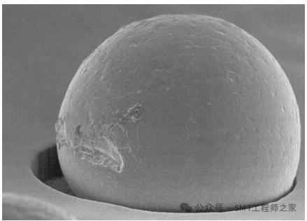
In their initial state, the eutectic solder balls on the BGA are shiny and relatively round. The connections, handling, and subsequent operational steps of the BGA may lead to deformation, damage, punctures, and dents.
Deformation of solder balls during testing and aging is an expected phenomenon, as long as it does not affect the usability of the product, anomalies are acceptable. There are many competing contact designs in the market vying for better market share. Each contact leaves a unique imprint on the solder balls. During testing and aging, these probes contact different positions on the solder balls, leaving unique imprint characteristics of each contact design on the solder balls.
It is known that solder balls can fall off in certain cases. The issue is not to visually detect whether solder balls are missing or damaged during testing, but to carefully optimize the solder connections and select test sockets that fit well with the device under test.
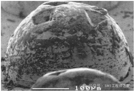
Some contacts only affect the sides of the solder balls rather than the bottoms, with the bottoms not being touched during contact. The following image illustrates such an example.
Other contacts will affect the bottoms of the solder balls. The following image shows solder balls being contacted at the bottom. The problem is that during reflow soldering, the flux may be trapped by the depressions left by the contacts, and under reflow heating, it may explode, causing solder to splatter and leading to short circuits and other issues.
Some contact designs can prevent flux entrapment. The contact probes create a pattern that serves as a channel for flux discharge when contacting the bottom of the solder balls, ensuring that flux is not trapped during reflow soldering.
Other contact impressions allow for flux entrapment. If a small hole forms in the bottom of the solder ball due to the impression, the likelihood of flux entrapment increases significantly. Flux trapped in shallow depressions may not cause issues. Damage problems only occur when the depression is larger than expected and holds enough flux.
Some contacts are designed with force mechanisms for each contact probe, while others have the same force mechanism acting on all probes. All different types of contact mechanisms will leave some imprints on the solder balls. The size of the contacts should match the size of the solder balls being tested to reduce solder ball deformation. Therefore, the size of the contacts needs to decrease as the solder ball size and array pitch decrease. Oversized contacts can cause short circuits or subject the solder balls to unintended levels of deformation.
The force mechanisms of the probes must match the hardness of the solder balls, which depends on the solder material composition. Excessive force can lead to unnecessary deformation. The force mechanisms need to provide enough force to contact the smallest solder balls in the array. When exposed to high temperatures for extended periods, solder balls will soften. The design of the force mechanisms must take this change into account to ensure they can be used in environments with temperature variations. Even at room temperature, continuous testing of components can increase the temperature at the contact points.
In practice, it is required that solder balls remain solderable after undergoing rigorous testing and aging, with their solder joints needing to have acceptable contact strength, contact area, and solder column shape. To assess the impact of testing and aging operations, items to observe include solderability, coplanarity, and the overall appearance shape of the solder balls. Solder balls should not lose excessive solder during testing and aging to ensure sufficient solder for optimal connections. Solder balls should be suitable for reflow soldering processes to form acceptable contact connections. Corrosion of solder balls and foreign materials introduced during aging and testing should not adversely affect the quality and long-term reliability of the solder balls. After testing and aging cycles, especially for non-melted solder balls, meeting the expected coplanarity is a fundamental requirement for good BGA connections to the substrate.
Different technologies have different contact points with the solder balls. In fact, the vast majority of contact designs are bottom contacts, forming connections by contacting the bottom of the solder balls. Given these options, it cannot be stated that certain parts of the solder balls are untouchable during operation. If there is no impact on the solderability, coplanarity, solder volume, quality, and reliability of the finished product, it is neither practical nor necessary to keep certain areas of the solder balls untouched.
3. Bare Board Testing
When considering the increasingly complex testing, inspection, and measurement of substrate interconnections, especially when it involves the electrical evaluation of the substrate, many issues arise. To reduce manufacturing costs while ensuring the electrical functionality of substrate interconnections, customers need to provide predefined test data in advance (preferably 100% netlist testing). The compatibility of this data is currently also an issue, and it is hoped that the industry will help resolve this through standardization efforts in the foreseeable future. A key issue in achieving this goal has proven to be the acceptance standards for the base grid pitch, which allows test equipment and socket manufacturers to verify and focus on innovations in universal solutions.
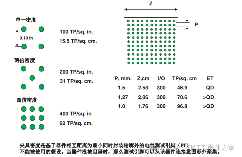
Using fixtures and probe beds for open and short circuit testing quickly becomes inadequate as the probe dimensions decrease and density increases. A test probe bed with double density or a pitch of 1.77mm seems sufficient to meet the requirements for pitches of 400μm or more. When the substrate density increases to pitches less than 400μm, alternative technologies need to be considered. A quadruple density fixture is a viable option (62 probes per square centimeter), but concerns about potential shape damage caused by probe contact are also increasing. Additionally, considering the costs of double or quadruple density fixtures and test equipment, adjusting the total test coverage within the expected cost has become difficult based on the current understanding of electrical testing and the linear projection of testing concepts.
For various grid partitions with I/O densities ranging from 200 to 1000, it is clear that double or quadruple density is suitable for this average I/O requirement for bare board continuity testing. However, if components are stacked in an “edge-to-edge” manner, testing using this method becomes impossible. This is because a BGA with a pitch of 1.0mm contains 96 pads per square centimeter, while a quadruple density test fixture can accommodate only 62 probes per square centimeter. Spreading components across the mounting structure can reduce some complexity but also consumes more space and reduces performance. It should also be noted that if the current testing concepts are used, achieving full coverage testing will require multiple tests or dual fixture testing, and maximizing component I/O will significantly increase the testing costs of bare boards. Figure 6-30 shows the relationship between component pad requirements and fixture performance.
Depending on the yield of the substrate being manufactured, flying probe testing eliminates the need for expensive fixtures, making it a cost-effective alternative to probe bed testing. Depending on the equipment used, probe bed testing is relatively slow, and the equipment may be quite expensive, a problem compounded by increased density requirements and additional network testing demands. Most of this equipment/testing technology has evolved alongside the semiconductor industry and has faced challenges from mechanical factors such as larger panel sizes. Additionally, in some cases, detecting small feature sizes can cause the detection system to fail, as it is difficult to energize such features with flying probes. If this technology is to be used for future complex substrates, additional equipment development will be necessary.
As the size of through-holes continues to decrease, traditional metallographic micro-section evaluation methods are limited, making this approach less feasible. For a typical micro-section laboratory, 150μm through-holes are practically a limit. If manufacturers want to understand more about the plating conditions of through-holes beyond just continuity, they need to seek alternative testing methods. Some manufacturers are now using electrical interconnect stress testing (IST) to measure the integrity and reliability of the holes.
4. Component Testing
The testability design of printed board components typically involves system-level testability issues. For most applications, there are requirements for system-level fault isolation and system recovery, such as mean time to repair, uptime percentage, individual fault duration, and maximum repair time. To meet these contractual requirements, system designs need to include testability features, which can often enhance PCBA-level testability. The concept of testability for printed board components must also align with overall integration, testing, and contract maintenance plans. When printed circuit board components require conformal coating, factors such as the testing equipment used in the factory, how integration and testing are planned, testing capabilities in warehouses and on-site, and the technical level of staff are all essential considerations when developing testing strategies for printed circuit board components.
The testing concepts applied at different stages of a project vary. For example, the first article debugging concept may be entirely different from the concept for testing spare parts after all systems have been shipped. Before starting the design of printed circuit boards, the functional requirements for system testability should be raised during the conceptual design review. These requirements and any derived requirements should be broken down into various printed board components and documented. The testing standards at the system and project levels and how these standards are broken down into printed board component requirements exceed the scope of this standard.
Functional testing and in-circuit testing are the two basic types of testing used for printed circuit board components. Functional testing is used to test the functionality of the electrical design. Functional testing equipment connects to the circuit board through connectors, test points, or probe beds. The functional testing of the circuit board is performed by applying predetermined signals (vectors) to the input of the printed circuit board component while monitoring the output of the printed circuit component to ensure the design responds correctly. In-circuit testing is used to detect manufacturing defects in printed board components.
In-circuit testing (ICT) accesses the board under test using a probe bed fixture that contacts each node of the printed circuit board component. The testing of printed circuit board components is completed by measuring all components on the board individually. In-circuit testing has few limitations for design. Conformal coated printed board components and many SMT components, as well as mixed technology printed board components, may have physical access issues with probe beds, thus limiting in-circuit testing. The main focus of in-circuit testing is that the pads or pins (1) must be on the grid (compatible with probe bed fixtures) and (2) should be accessible from the back side of the printed circuit board component (i.e., the non-component side or the solder side of through-hole technology boards).
The manufacturing defect analyzer (MDA) is a low-cost alternative to traditional in-circuit testing equipment. Like ICT, MDA can check for defects in the structure of printed circuit board components. It performs a series of tests, primarily to check for short and open circuit issues in printed board components without applying power. For high-volume production with highly controlled processes (such as statistical process control techniques SPC), MDA can serve as a viable method for testing printed circuit board components. Non-vector testing is another low-cost alternative to in-circuit testing devices. Non-vector testing seeks to identify SMT board device pin failures related to the manufacturing process without requiring programming of test vectors. This is a non-powered measurement technique, primarily consisting of three basic test types:
-
Analog node testing—using ESD protection diodes on most digital or mixed-signal device pins to measure DC current on unique pin groups of the printed board component.
-
RF induction testing—using device protection diodes on the printed board component, magnetic induction is often used to test device failures. This technique uses the power and ground pins of the chip to detect open solder joints, bond wire damage, and device failures caused by ESD, and incorrect component installation direction can also be detected. This type of testing requires fixtures containing magnetic sensors.
-
Capacitive coupling testing—this technique uses capacitive coupling to test for open pins. It does not rely on the internal circuits of the device but rather on the metal lead frame present in the device to test the pins. The correctness of connectors and sockets, lead frames, and capacitor polarities can be detected using this technique.
1. Circuit Board Bending During Testing
Due to lead-free solder joints being stiffer and less ductile than tin-lead solder joints, if the design and manufacturing lead to excessive bending of the board during use, ICT/functional testing fixtures can damage the solder joints. Damage caused by this bending is typically due to improper support and downward pressure locations on the circuit board, especially around densely populated probe areas. Excessive bending of the circuit board can also be caused by misalignment of the support plate and the downward pressure plate, excessive probe pressure, excessive or insufficient vacuum, or improper distribution of springs between the upper plate and the probe bed. Additionally, poorly designed tooling fixtures can easily lead to abnormal bending of the PCB, resulting in damage.
To ensure that testing fixtures do not damage printed circuit assemblies (PCAs), strain and strain rate measurements must be taken during the use of the testing fixtures. Strain measurements should be taken at the corners of the BGA using a triaxial strain gauge placed according to the IPC/JEDEC9704 standard. Strain and strain rate should be specified in the “strain limit specification,” which defines the requirements for loading, testing, and releasing the product under test (UUT).
• The strain measurement system must be capable of sampling all strain gauge directions (e1, e2, e3) simultaneously to accurately measure and calculate all strain components.
• In the axial or diagonal direction, the acceptable strain limit for tin/lead PCAs is 600με.
• In the axial or diagonal direction, the acceptable strain limit for lead-free PCAs is 450με.
• In the axial or diagonal direction, the typical strain rate limit is 30000με/s.
• The typical damage acceptance standard is: using cross-section failure analysis (FA) methods, no damage to BGA solder joints is found.
2. In-Circuit Testing Issues
In-circuit testing can detect open circuits, short circuits, component misplacements, component inversions, device failures, incorrect assembly of printed circuit board components, and other manufacturing defects. In-circuit testing cannot identify components that are on the edge of acceptable status, nor can it verify critical timing parameters or other electrical design functions.
In-circuit testing of digital printed board components involves a process known as reverse driving (see IPC-T-50). Reverse driving can also lead to device oscillation, and the testing equipment may cause the device to be in a non-saturated state due to insufficient driving. Reverse driving can only be performed under time-controlled conditions; otherwise, device nodes (with excessive drive outputs) may overheat.
When designing printed boards and printed board components, two points that need to be considered regarding online testability are the compatibility of in-circuit testing fixtures and electrical design considerations.
3. Functional Testing Issues
Some issues related to functional testability arise when designing printed board components. Using test connectors, synchronization and initialization issues, long counter chains, self-diagnostic functions, and physical testing are topics that will be discussed in detail in the following chapters, but this does not mean that this article is a tutorial on testability; it merely provides ideas on how to address common functional testing issues. Fault isolation for conformal coated boards or most SMT boards and mixed technology boards is very difficult due to the lack of circuit access points on the board. If important signals can be routed to test connectors or detectable areas on the printed board (test points), fault isolation will be significantly improved. This will reduce the costs of detection, isolation, and troubleshooting. A circuit can also be designed so that test connectors can be used to stimulate the circuit (e.g., using test connectors as a data bus) or shield the functionality of printed board components (e.g., shielding self-oscillators and adding single-step operation functionality through test connectors).