eMMC, or Embedded Multi Media Card, is defined by the MMC Association. The concept of an embedded multi-media card may be unfamiliar to many. Let’s start by understanding it literally. Since there is an embedded multi-media card, shouldn’t there be a multi-media card?
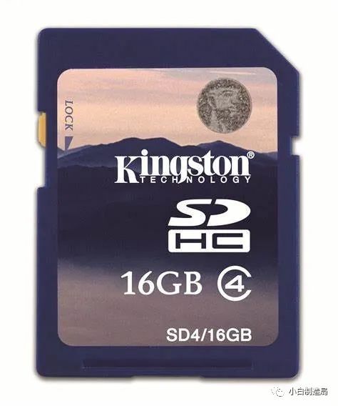
Exactly, you are correct. Moreover, there is a type of card that has developed based on this concept. It is the SD card. Many people should be familiar with this type of card. We have encountered it in cameras we once loved, during the era when USB drives were prevalent, and when smartphones were not as ubiquitous as they are today; we also referred to it as an SD card. It looks like this.
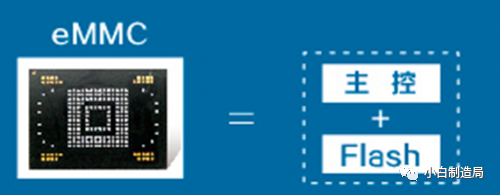
eMMC, simply put, is the integration of the MMC component into a standard BGA package, looking like an SD card in a different encapsulation form, yet there are design differences. We will discuss BGA packaging in future chapters. So, what components does the MMC consist of?
In simple terms, eMMC is an initial embedded product formed by NAND FLASH + Controller + Multi-Media Interface. It was created to simplify the use of memory in digital devices, integrating FLASH and the controller into a single chip, aligning with the current trend of integration. Additionally, eMMC has implemented FLASH management technologies, including error detection and correction, FLASH wear leveling, bad block management, and power loss protection.
The interface speed of eMMC can reach up to 52 MBytes per second, offering fast and upgradeable performance, with interface voltages of either 1.8V or 3.3V.
eMMC has three main advantages:
-
Simplifying Device Memory Design:
eMMC is currently the most popular local storage solution for mobile devices, aimed at simplifying device memory design. Since the design of NAND Flash chips depends on the product and technical characteristics of the manufacturers, there has been no technology that can be universally applied to all brands (such as Samsung, KingMax, Toshiba, or Hynix, Micron).
-
Accelerating Product Development Speed:
Each time NAND Flash manufacturing technology evolves, from 70nm to 50nm, and then to 40nm or 30nm, manufacturers must redesign. According to Moore’s Law, semiconductor process technologies are updated every 2 years, and developing applications based on NAND Flash requires significant effort to study different manufacturers’ technical characteristics, which consumes a lot of time and energy.
The design concept of eMMC is to simplify the use of device memory. By designing the NAND Flash chip and control chip into a single MCP chip, device customers only need to purchase eMMC chips (which are implemented by specialized third parties), integrate them into new devices, and do not need to deal with complex NAND Flash compatibility and management issues. The biggest advantage is that it shortens the product launch cycle and R&D costs, accelerating the pace of product innovation.