To facilitate rework, it is recommended to provide sufficient spacing (3mm to 5mm) around the BGA. It is advisable to adopt the upper limit of the spacing, especially when CBGA uses a stepped stencil for solder paste deposition and when hot air is used for rework. However, if a diode laser system is used for rework, the spacing requirement can be reduced to 0.5mm to 1.0mm, as laser rework does not affect adjacent components.
1. Mounting Requirements
The advantage of BGA packaging over other advanced high lead count packages (fine pitch, TAB, PGA, etc.) lies in its compatibility with existing surface mount equipment. The self-alignment capability of BGAs makes them more tolerant during the mounting process.
2. Repair/Rework Requirements
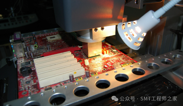
The requirements for component spacing primarily stem from the need for repair/rework of BGA components. A typical BGA rework method involves five steps:
1) Heat the solder joints to reflow temperature to remove the package; 2) Remove and clean residual solder from the BGA connection pad pattern; 3) Apply new solder paste or flux; 4) Mount the new BGA package; 5) Heat the solder joints to reflow temperature to assemble the BGA device onto the PCB.
Each step in the above process may require the establishment of isolation zones. Rework equipment manufacturers provide specific details regarding the necessary isolation zones, with general rules outlined as follows:
Almost all hot air methods use nozzles directed downward towards the BGA and/or heat the solder joints around the BGA to facilitate removal and reflow. The recommended component isolation zone should be set at a distance of 2.5mm from the outer edge of the hot air nozzle. If the nozzle size is included, it should be 3.8mm away from the component body. The spacing around the BGA provides room for the nozzle and reduces the risk of heating adjacent component solder joints above reflow temperature. When using a laser system for rework, the isolation zone can be reduced to less than 1mm.
During repair, after the BGA package is removed from the PCB, the connection pad must be cleaned, and new solder paste or flux must be applied before placing the new component. If solder paste or flux is applied manually, or if solder paste is applied using an automated spraying system, no special component isolation zone is required. However, many repair systems use small stencils and scrapers to manually apply solder paste to the PCB connection pads or the device’s solder balls, generally requiring a minimum component isolation zone of 3mm (i.e., the nominal distance between adjacent component bodies) to meet the nozzle spacing requirements and the small stencil requirements when printing onto the PCB connection pads. If there are large adjacent components, a much larger minimum distance may be necessary.
3. Overall Layout
There are no specific overall layout requirements for BGAs. However, it is recommended not to place them near the centerline of the PCB. This approach can reduce potential coplanarity issues caused by warping of the PCB during the reflow process. Additionally, BGA packages should not be placed near large through-hole components, as this can cause the PCB to tighten and significantly increase local stress on the corner solder joints of the BGA. In some cases, if the strain induced at the BGA corners can be reduced by the stiffness of nearby through-holes or other components, certain features may be utilized to effectively protect the BGA. Finally, BGA packages should not be placed in the same diagonal line as mounting brackets, standoffs, and screws used to support and secure PCB components, as this can more easily induce stress levels that damage the corner solder balls.
4. Alignment Markings (Silkscreen, Copper Markers, Pin 1 Identifier)
It is recommended to print alignment marks for the BGA package on the PCB to verify whether the components are aligned before and after reflow. BGAs, especially PBGA, can automatically align even with up to 50% offset of the connection pads during the reflow process. Therefore, any mentioned offset typically refers to a connection pad diameter length or even more.
Alignment markings help visually check whether the component placement is sufficiently accurate. Silkscreen ink and copper are the two main materials used for alignment markings. Silkscreen ink is the most common material, but it requires additional processes in PCB manufacturing. Copper alignment markings are manufactured simultaneously with other copper patterns, thus providing more precise positioning. High-speed lines may be affected by ungrounded copper in this scheme, as unconnected copper conductors can accumulate into a dissipative and uncontrollable capacitance.
In many cases, the markings used for equipment or operators are employed to assess the BGA alignment check during the placement operation. For peripheral lead components, reference points have been standardized, allowing the placement machine to adjust the placement head accordingly to improve the final component positioning accuracy.
Local reference points are usually arranged diagonally to allow for adjustments in the θ angle, and many placement tools and equipment have integrated this technology. Using reference points may not provide the most obvious status for inspection, but most inspectors can roughly estimate whether the package has been correctly placed between the two reference points, thus verifying their position. In some cases, manufacturers may need to use angle brackets instead of reference points to assist the human eye in making judgments; however, cameras on placement machines are often not familiar with such structures, making this not the most suitable method for automated assembly. (See the image below)
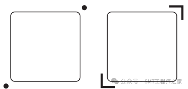
By using silkscreen, the overall profile of the package can be outlined for visual alignment. Another common alignment pattern marks only the corner areas of the BGA, with corner markings being only 0.8mm long on each side. Copper can also be used as corner markings, as it does not interfere with routing as long as it does not affect circuit performance (e.g., causing unwanted capacitance).
All alignment markings need to be at least 0.25mm away from the outer edge of the BGA package, providing sufficient clearance for viewing the markings around the BGA package. A Pin 1 identifier is required on the BGA connection pad pattern. This identifier can take the form of an insertion symbol, dot, or other easily distinguishable shapes. The material for the Pin 1 identifier can be silkscreen ink or copper, and the resolution must be high enough to avoid confusion with other markings around the connection pad pattern.