
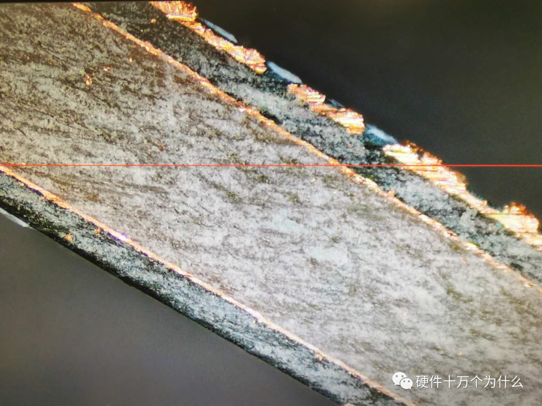
The image below marks the position of the DDR2 chips that were cut open. We can see that there are dense traces inside the new foam. The BGA solder balls are marked in red. This is a 6-layer board, with the positions of the TOP, BOTTOM, and the four internal electrical layers already indicated. Since the cut was not very vertical, the three vias on the left are incomplete, while the one on the right is relatively intact.

Between the copper layers is a fiber board, and between the top layer and the first power layer (GND layer), between the two middle board layers, and between the second power layer (VCC layer) and the bottom layer is a glass fiber board, usually made of FR-4 material, forming a double-sided board. After these three double-sided boards are completed, they are bonded together with a bonding board (also usually made of FR-4 material) to form a six-layer board.

Below is a cross-section of a 4-layer board. It can be seen that the solder mask layer is black, not green.
Click the video to see the cutting process:
Even the ceramic capacitors were cut open!
Cut across, then grind a bit, and polish!

The basic structure of a simple parallel plate capacitor consists of an insulating intermediate dielectric layer plus two external conductive metal electrodes. Structurally, the MLCC is a multilayer stacked structure; simply put, it is a parallel combination of multiple simple parallel plate capacitors.
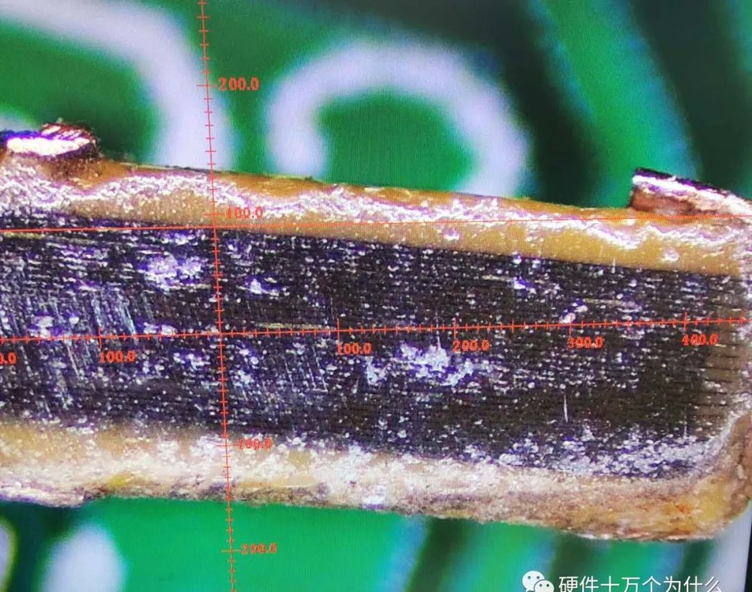
The outermost layer is the electrode, and since the end face has been ground off, only a ring remains around the sides. In the middle, the two side electrodes are stacked together, and the dark brown in the center is the ceramic, i.e., the dielectric.
The inductor was also cut open!

Solid aluminum capacitor

Tantalum electrolytic capacitor
