Understanding the Past and Present of PCB Circuit Boards
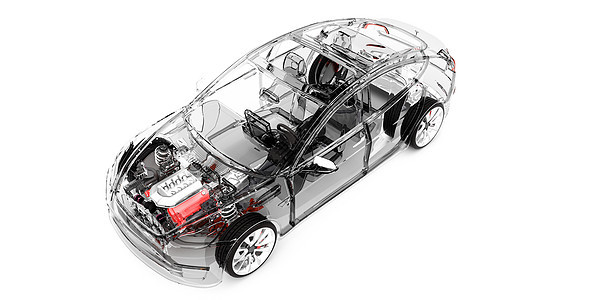
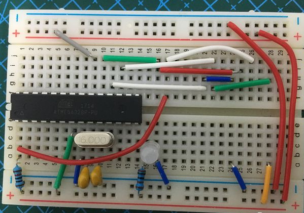
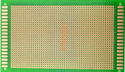
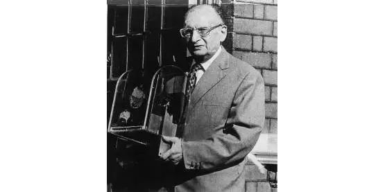
When it comes to circuit boards, many people should be familiar with them, as they are ubiquitous in our lives, from small devices like Bluetooth headsets, electronic watches, and calculators to larger systems like computers, communication devices, and military/aerospace systems. Wherever integrated circuits are needed, they rely on PCB to carry electronic components.Before PCB appeared, electronic components were directly connected with wires. In devices with a large number of components, the wiring often became chaotic, posing significant safety risks and leading to errors.Or one could use universal PCB boards, commonly known as perforated boards.So how was this great circuit board created?Paul EislerThis brings us to the “Father of PCB,” Austrian Paul Eisler. In 1936, Paul Eisler first used printed circuit boards in radio devices.Eisler developed the concept of using etched foil to record traces on a substrate. Initially, no one really paid attention to this invention, but by 1943, for the timing devices of bombs, Americans began using printed circuits as fuses, which started to see widespread application. Americans also applied it to military radios.Since then, circuit boards have gained a great reputation….and have continued to develop…In 1948, the United States officially recognized this invention for commercial use.By the early 1950s, the copper foil etching method became the mainstream PCB manufacturing technology, starting the production of single-sided boards.In the 1960s, metallization of holes in double-sided PCB began large-scale production.In the 1970s, multi-layer PCB rapidly developed, continuously moving towards high precision, high density, fine lines, high reliability, low cost, and automated continuous production.In the 1980s, surface mount printed boards (SMT) gradually replaced through-hole PCB, becoming the mainstream of production.Since the 1990s, surface mount technology has further developed from quad flat packages (QFP) to ball grid array packages (BGA).Since the 21st century, high-density BGA, chip-scale packaging, and organic laminate materials for substrate multi-chip module packaging printed boards have seen rapid development.
01
The Development History of Circuit Boards in China
In 1956, China began research on PCB.In the 1960s and 70s, single-sided boards began mass production, but at that time, due to various factors, the development of printed board technology was slow, causing the entire production technology to lag behind advanced levels abroad.By the 1980s, advanced single-sided, double-sided, and multi-layer printed board production lines were introduced from abroad.Entering the 1990s, manufacturers from Hong Kong and Taiwan began to invest in factories on the mainland, leading to a rapid increase in production and technology in China.By 2002, China became the third-largest producer of PCB.Known as the “mother of electronic components,” PCB has eliminated traditional complex wiring, reduced the connection and soldering workload between electronic components, minimized the overall size of devices, lowered production costs, and improved the quality and reliability of devices. In short, the future of PCB is promising!Copyright Statement:This article is copyrighted by the original author and does not represent the views of the association.The articles pushed by the “Jiangxi Province Electronic Circuit Industry Association” are for sharing purposes only and do not represent the position of this account. If there are copyright issues, please contact us for removal.