Unstable Chip Programming? You Might Have Overlooked These
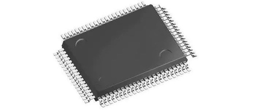
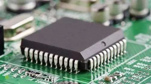
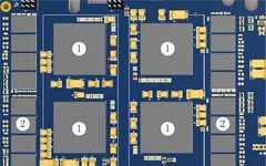
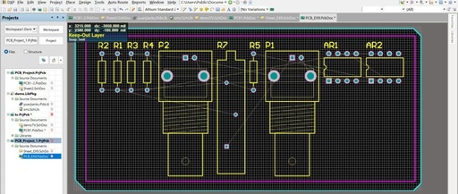
Online programming is favored by many users due to its advantages of integrated programming and testing. However, it often suffers from instability and high programming failure rates due to long wiring caused by connection fixtures and clamps. How can we improve this? Figure 1: Online Programming Fixture 1Increase Shielding Layer to Prevent Electromagnetic and Static … Read more