The wiring formation process should include a formal design evaluation of the wiring details, with participation from as many relevant departments as possible within the company, such as manufacturing, assembly, and testing. The wiring scheme approved by representatives from the affected departments ensures that production-related factors have been considered in the design. The success of the interconnection structure design depends on many interrelated factors. From the perspective of the end product’s use, the following common parameters should be considered for their impact on the design. Other design for manufacturability issues include:
- Environmental conditions, such as ambient temperature, heat generated by components, ventilation, shock, and vibration.
- If components are maintainable and repairable, considerations must include component/circuit density, selection of circuit board/coating materials, and accessibility for component installation.
- Factors that may affect the size and position of mounting holes, connector positions, lead protrusion limits, component placement, brackets, and other hardware placement interfaces.
- Factors that may affect testing/troubleshooting requirements for component placement, wiring, and connector contact distribution.
- Process margins such as etching factor compensation, used for line width, spacing, and connection pad manufacturing.
- Manufacturing constraints such as minimum etching profiles, minimum plating thickness, printed board shape and size, etc.
- Coating and marking requirements.
- Assembly techniques used, such as surface mount.
- Through-hole and mixed technologies.
- Printed board performance levels.
- Material selection.
- PCB component manufacturability based on manufacturing equipment constraints.
- Flexibility requirements.
- Electrical/electronic performance requirements.
- ESD sensitivity considerations.
1. Design of In-Process Boards/Fixtures
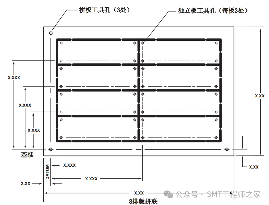
In-process board assembly and fixtures are standard processes for testing and assembly. In-process manufacturing requires a reference system, and each individual board or fixture in the process also needs its own reference system. To reduce the accumulation of tolerances, it is important to associate the reference of each individual board with the in-process board reference. (See the diagram below)
Most assembly plants prefer to use fixtures for assembly, as shown in the diagram below. These fixture manufacturers will position them on a standard in-process board, which is typically 460×610mm. Designers are encouraged to collaborate with manufacturing suppliers to optimize material flow, the separation methods of fixtures/individual boards, and how testing will be conducted.
2. Intermediate Process/Final Product Test Fixtures
Test fixtures, used in the industry for many years, are designed to evaluate in-process products. These test fixtures can represent the characteristics of printed boards or components, and they are integrated into the edges of the in-process board for use by PCB manufacturers or integrated into the edges of fixtures for use by assembly manufacturers. Most PCB manufacturers and assembly plants have their own control processes. However, testing fixtures through various physical evaluation methods is valuable for determining whether the processes and methods used to produce that component are in a controlled state that meets requirements. This concept is essential for BGA, as the connection pads or solder joints are not visible after assembly. Test fixtures or samples should reflect the specific characteristics of the printed board or in-process board. Data derived from the in-process board should be used to establish requirements for vias and connection pads, line widths, spacings, etc. When samples are used to establish process control parameters, they should continuously use a single hole dimension or connection pad structure that reflects this process. Process characteristics and overall characteristics of the printed board should match each other.
IPC-2221 provides excellent test fixtures for evaluating these printed board and component characteristics. They include:
- Hole solderability
- Solder mask
- Thermal stress plating
- Thickness and connection strength
- Plating adhesion
- Surface solderability
- Solder mask
- Surface mount solderability
- Surface bonding strength
- Surface insulation resistance
- Moisture and insulation resistance
- Positioning
- Interconnection resistance
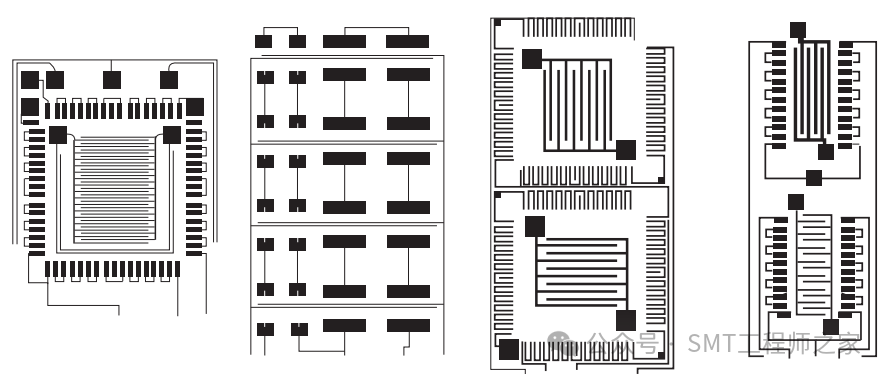
The diagram below shows an alternative test fixture commonly used to assess the cleanliness of solder boards after solder ball connections are completed. These comb-shaped patterns used on printed boards are designed to determine whether flux or flux residues will impair the electrical performance of the product.