The design of BGA (Ball Grid Array) on PCB boards is very common in the industry, and the issue of irregular BGA sizes can severely affect the soldering quality and electrical performance of PCBs. To effectively improve this issue, it is necessary to address it from the aspects of design and manufacturing processes.1. Package Design1. Solder Pad Size and Shape: Preferably use round and oval solder pads, avoiding designs with sharp corners and irregular shapes. The size of the pads should be designed as large as possible, considering the package size and overall PCB layout, as smaller BGA sizes (for example, less than 0.25MM) significantly increase the likelihood of irregular processing.2. Solder Mask Opening Design: The solder mask openings should be refined, with different designs for BGA solder points that are independent, on copper pads, or have connection line ends. The size of the solder mask opening should be slightly larger than the pad size, but not excessively so, with an increase of 0.05-0.1MM on each side being optimal.3. Use Solder Mask ON PAD design to regularize the shape and size of the pads based on the size of the solder mask openings.#PCB Information on Solder Mask ON PAD Design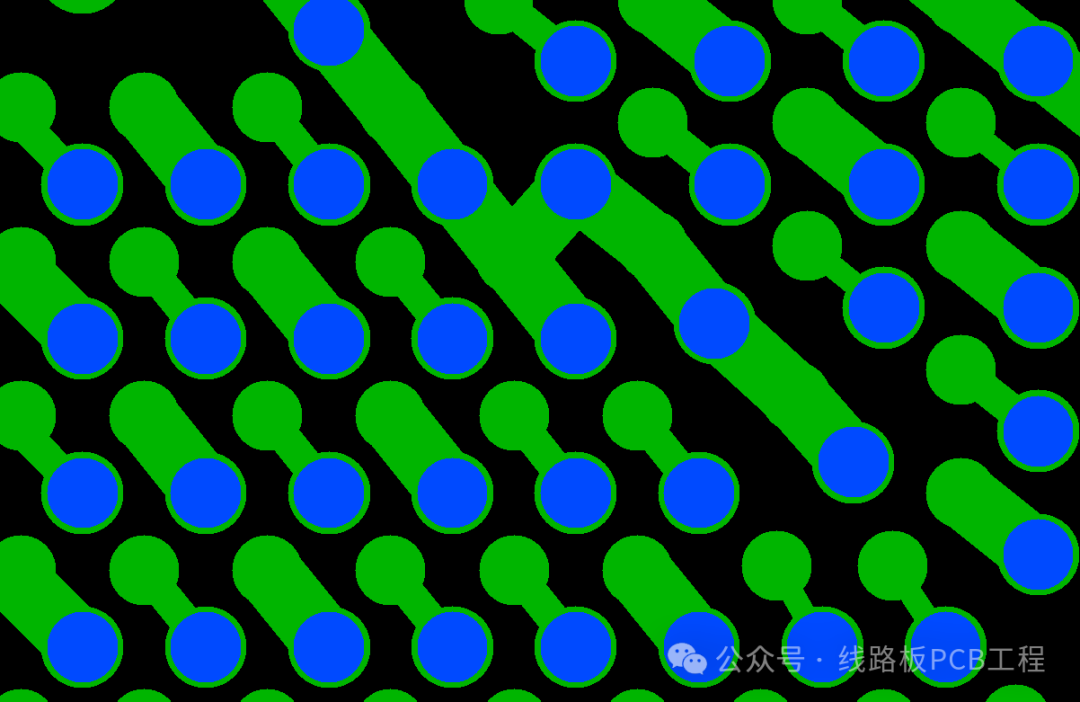 2. PCB Engineering Data Optimization1. Solder Point Compensation Pre-Adjustment: Compensation should be made as optimally as possible according to the etching capabilities, with differences in compensation for independent points and different positions on copper pads. For independent points, compensation can be slightly increased, while for copper pads, it should be reduced (specific adjustments depend on the etching capabilities of each manufacturer).2. Solder Mask Opening Optimization: Different treatments should be applied to BGA solder mask openings at various locations such as copper pads, independent points, and necks of connection lines. For example, the size of solder mask openings on copper pads should be reduced to maintain consistency with independent points, while the openings at the connection line ends should be treated accordingly. Through these adjustments, ensure that the solder mask opening sizes perfectly match the pads.
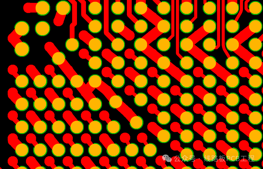 3. PCB Manufacturing Process Optimization1. Use advanced PCB graphic processing equipment, such as fully automatic LDI exposure machines, which, compared to traditional CCD exposure machines, do not require manual alignment, thus avoiding human operational errors. The processing accuracy can reach the micron level, allowing precise control of the size and position of BGA solder point graphics, effectively reducing irregular solder point issues caused by exposure deviations.2. The solder mask process is also crucial for the quality of BGA solder points. Using fully automatic solder mask LDI exposure machines can achieve high-precision processing of solder mask graphics. This equipment, through digital control, can accurately control the size, shape, and position of solder mask openings, offering higher processing precision and stability compared to traditional screen printing processes. Additionally, automated operations reduce human interference, effectively avoiding issues such as solder mask misalignment and inconsistent opening sizes.3. Etching Process Optimization: Etching is a key process affecting the dimensional accuracy of BGA solder points. By optimizing the etching solution formulation, precisely controlling etching temperature and time, and improving the uniformity of equipment spraying, the controllability and consistency of the etching process can be enhanced. For example, using dynamic etching technology, etching parameters can be automatically adjusted based on the thickness of copper foil in different areas, ensuring that BGA solder points maintain stable dimensions and regular shapes during the etching process.