Five Typical Failure Phenomena in Chip Packaging

Five Typical Failure Phenomena in Chip Packaging

Source: Learning About Things Original Author: Xiao Chen Po Po This article introduces the five typical failure modes in chip packaging: gold wire displacement, chip cracking, interface cracking, substrate cracking, and reflow soldering defects. In the field of integrated circuit packaging failure analysis, gold wire displacement, chip cracking, interface cracking, substrate cracking, and reflow soldering … Read more

Photonics Chips Challenge Nvidia’s NVLink

Photonics Chips Challenge Nvidia's NVLink

According to executives interviewed exclusively by EE Times, startup chip manufacturers Celestial and OpenLight are set to produce their first chips this year, providing faster photonics and lower power consumption for large-scale customers running AI data centers, such as Amazon, Microsoft, and Google. In August, Celestial secured $255 million in funding from TSMC’s VentureTech Alliance … Read more

Future Development Trends in the Chip Packaging Industry

Future Development Trends in the Chip Packaging Industry

The chip packaging industry is at a crossroads in the “post-Moore’s Law era.” Based on the latest information from multiple authoritative organizations and industry leaders for 2024-2025, the future development trends over the next 5-7 years can be summarized with “six key terms + three roadmaps.” Keyword 1: System-Level Ultra-Large Packaging (SLP/CoPoS) • In 2025, … Read more

Steps and Advantages of Chip Packaging Technology

Steps and Advantages of Chip Packaging Technology

ClickFollow “Semiconductor New Materials Industry” at the top,Click “❤” and “” and share Addthe editor on WeChat to find like-minded individuals in the industry If you have a chip that needs to be fixed onto a circuit board or other substrate to ensure normal output of the chip’s performance, the three most common methods are: … Read more

How to Query the Wafer Origin Information of STMicroelectronics Chips?

How to Query the Wafer Origin Information of STMicroelectronics Chips?

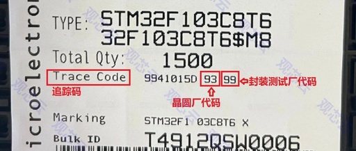
When declaring chips for customs, customs usually requires the provision of wafer origin information (Wafer Origin). However, many people find that the official website of STMicroelectronics does not directly provide this information. So, is there another way to accurately determine the wafer origin of the chip? The answer is: you can determine it through the … Read more

Detailed Explanation of Semiconductor Chip Packaging and Testing Process

Detailed Explanation of Semiconductor Chip Packaging and Testing Process

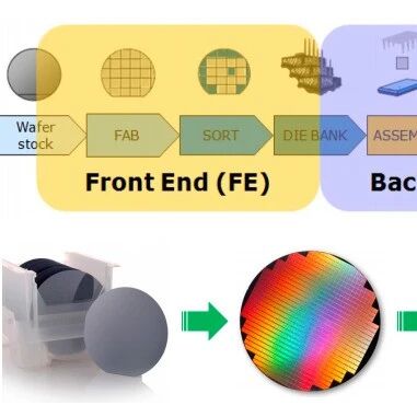
The chip packaging testing phase aims to process wafers that meet quality standards through precise cutting, wire bonding, and encapsulation processes to ensure electrical connections between the chip’s internal circuits and external devices, providing necessary mechanical and physical protection for the chip. Testing tools are used to conduct comprehensive and rigorous functional and performance testing … Read more

Understanding Chip Packaging Processes (Traditional Packaging)

Understanding Chip Packaging Processes (Traditional Packaging)

In the previous issue, we introduced some background knowledge about chip packaging:A Beginner’s Guide to Chip PackagingIn this issue, we will focus on the specific process of packaging.As previously mentioned, there are many forms of packaging, including traditional and advanced packaging.Different packaging types have different processes and techniques. After completing the entire write-up, I found … Read more

Cleanroom Requirements for Chip Packaging and Testing Areas

Cleanroom Requirements for Chip Packaging and Testing Areas

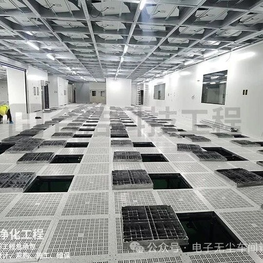
  The cleanliness requirements for chip packaging and testing areas vary based on specific process steps and product characteristics, typically ranging from ISO Class 5 (100-level) to ISO Class 7 (10,000-level). Below are the cleanliness level classifications and criteria for different areas; let’s explore this together with Hejie Technology Cleanroom Engineering Company! 1. Cleanliness Requirements for … Read more

Four Bonding Methods in Chip Packaging

Four Bonding Methods in Chip Packaging

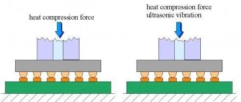
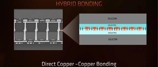
Chip packaging is a critical step in semiconductor manufacturing, providing physical protection, electrical interconnection, and heat dissipation for chips. Bonding technology is the method of connecting bare chips to external materials. Currently, there are four main bonding technologies: the traditional and reliable Wire Bonding, the high-performance Flip Chip Bonding, the highly automated Tape Automated Bonding … Read more

In-Depth Analysis of the Current State of China’s Chip Packaging Industry (Including Potential Companies)

In-Depth Analysis of the Current State of China's Chip Packaging Industry (Including Potential Companies)

Continuing from the previous discussion, we previously conducted an in-depth analysis of the upstream materials and chip design industry in China, recommending companies with potential for the future. In this issue, we will discuss the current state of China’s chip packaging industry. The Chinese chip packaging industry is currently at a bottleneck in development. Some … Read more