Comprehensive Guide to Advanced Semiconductor Packaging (Part 2)
Comprehensive Guide to Advanced Semiconductor Packaging (Part 2)

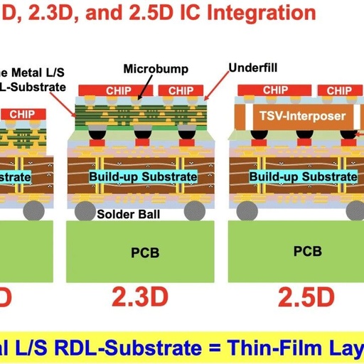
[Image]【Table of Contents】1. Electronic Packaging Overview 2. Early Packaging Types 3. 2D: Flip Chip Packaging 4. 2D: Wafer-Level Packaging 5. The Rise of Advanced Packaging 6. 2.1D/2.3D: Ultra-Thin Organic Interposers 7. 2.5D: Silicon Interposers, Microbumps, Silicon Through-Silicon Vias, and Silicon Bridges 8. 3D-IC Packaging 9. Hybrid Bonding 2.1D/2.3D: Ultra-Thin Organic Interposers (Inte…
Steps and Advantages of Chip Packaging Technology

Steps and Advantages of Chip Packaging Technology

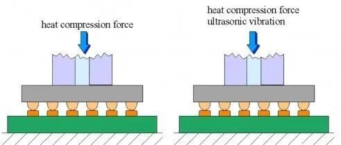
ClickFollow “Semiconductor New Materials Industry” at the top,Click “❤” and “” and share Addthe editor on WeChat to find like-minded individuals in the industry If you have a chip that needs to be fixed onto a circuit board or other substrate to ensure normal output of the chip’s performance, the three most common methods are: … Read more

Trends in Semiconductor Packaging and Testing Technologies

Trends in Semiconductor Packaging and Testing Technologies

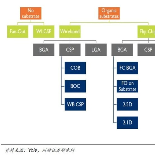
Follow our public account, click the top right corner of the public account homepage ” · · · “, set a star mark, and stay updated on the latest news in automotive semiconductors. There are many packaging forms for semiconductor devices, which can be classified into three categories based on their shape, size, and structure: … Read more

Bridging Chips and Circuit Boards – Packaging

Bridging Chips and Circuit Boards - Packaging

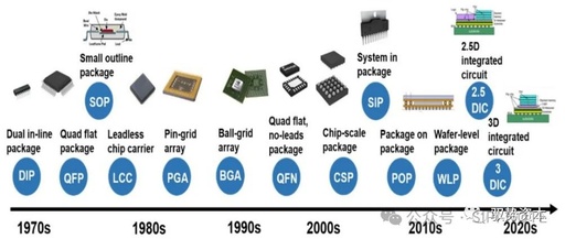
The development of packaging has evolved from the early DIP to the current 3D ICs [1][2], with a variety of packaging types emerging. Just the QF series has spawned a long list of types such as QFN (no leads), QFP (with leads)… There are many choices in terms of product applications [3], and each type … Read more