Avoid Layout Pitfalls! A Comprehensive Guide to Special Component Layout in PCBs
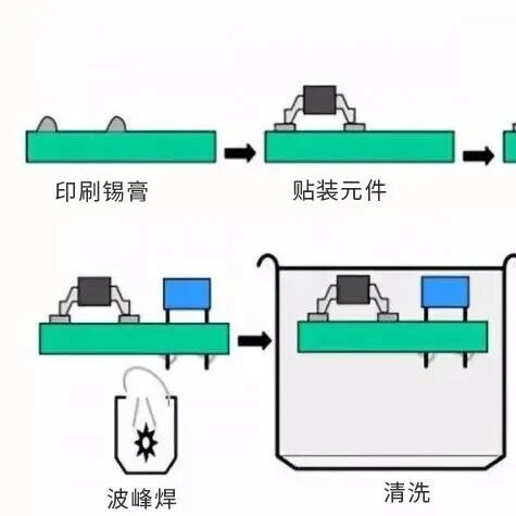
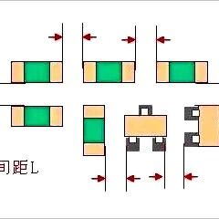
PCB component layout is not a matter of personal preference; it follows certain rules that must be adhered to. In addition to general requirements, some special components have different layout requirements. Layout Requirements for Crimping Components 1) For crimping components with bent male/female pins, there must not be any components higher than 3mm within 3mm … Read more