
When designing high-performance data acquisition systems, diligent engineers carefully selecthigh-precision ADCs and other components required for the analog front-end adjustment circuit. After several weeks of design work, they execute simulations and optimize the circuit schematic. To meet deadlines, designers quickly assemble the PCB layout and routing. A week later, the first prototype PCB is tested. Unexpectedly, the performance of the PCB differs from expectations.Has this scenario happened to you?Optimal PCB layout and routing are crucial for achieving the expected performance of the ADC.When designing circuits that include mixed-signal devices, it is essential to start with a good grounding arrangement and use optimal component placement and signal routing to separate the design into analog, digital, and power sections.The reference path is the most critical aspect of ADC layout and routing because all conversions are a function of the reference voltage. In traditional Successive Approximation Register (SAR) ADC architectures, the reference path is also the most sensitive due to the dynamic load on the reference pin from the reference source.Since the reference voltage is sampled multiple times during each conversion, high current transients occur at this terminal, where the internal capacitor array of the ADC is turned on and charged at this location. The reference voltage must remain stable during each conversion clock cycle and stable to the required N-bit resolution; otherwise, linear errors and code loss errors will occur.Figure 1 shows the current transients at the reference terminal of a typical 12-bit SAR ADC during the conversion phase.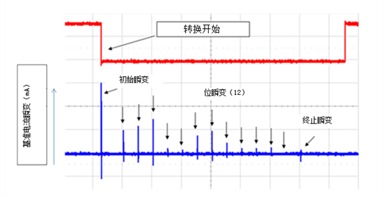 Figure 1. Current transients at the reference pin of a 12-bit SAR ADCDue to these dynamic currents, high-quality bypass capacitors (CREF) are required to decouple the reference pin. This bypass capacitor acts as a charge reservoir, providing instantaneous charge during these high-frequency transient currents. The reference bypass capacitors should be placed as close to the reference pin as possible and connected with short, low-inductance traces.Figure 2 shows an example of the PCB layout of the 14-bit dual ADC ADS7851 from TI, which has two independent internal voltage references.
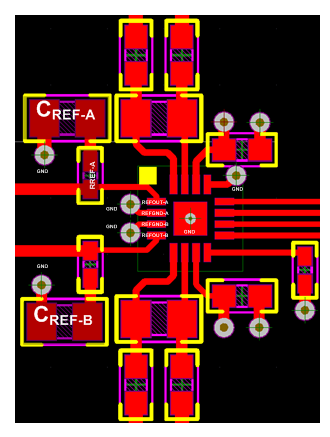 Figure 2. PCB layout example of a dual ADC with two independent internal voltage referencesIn this four-layer PCB example, the designer used a solid ground plane located directly beneath the components and divided the PCB into analog and digital sections to keep sensitive inputs and reference signals away from noise sources. He used a 10μF, X7R grade, 0805 size ceramic capacitor (CREF-x) to bypass the REFOUT-A and REFOUT-B reference outputs for optimal performance, connecting them to components using small 0.1 Ω series resistors to maintain low and constant overall impedance at high frequencies. He also used wide traces to reduce inductance.I strongly recommend placing CREF on the same layer as the ADC. Additionally, avoid placing vias between the reference pin and the bypass capacitors. Each reference ground pin of the ADS7851 has a separate ground connection, and each bypass capacitor has a low-inductance connection to ground.If you are using an ADC that requires an external reference source, you should minimize the inductance in the reference signal path—from the reference buffer output to the bypass capacitors to the ADC reference input.Figure 3 shows the layout example of an 18-bit SAR ADC ADS8881 using an external reference and buffer. By placing the capacitors within 0.1 inches of the pins and connecting them with 20 mil wide traces and multiple 15 mil ground vias, the designer kept the inductance between the reference capacitor and the REF pin below 2nH. I recommend using a single 10uF, X7R grade, 0805 size ceramic capacitor rated for at least 10V.The trace length from the reference buffer circuit to the REF pin should be kept as short as possible to ensure a fast and stable response.Proper decoupling of the REF pin is critical for achieving optimal performance. Furthermore, maintaining low-inductance connections in the reference path ensures that the reference drive circuit remains stable during conversions, bringing you one step closer to achieving the desired results.
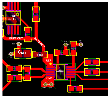 Figure 3. ADC layout example with external reference and buffer(This issue’s practical sharing group offers the “Selected Tips for Power Design” collection, welcome to join the group)