Considerations for Vias on PCBs
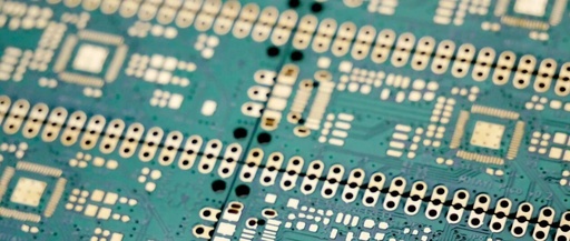
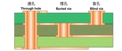
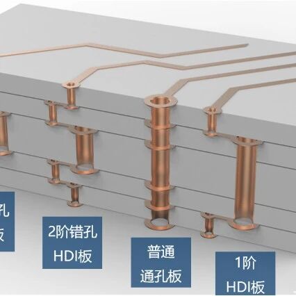
Vias are one of the essential components of multilayer PCB boards, with drilling costs typically accounting for 30% to 40% of the PCB manufacturing costs. Simply put, every hole on a PCB can be referred to as a via. Functionally, vias can be divided into two categories: One is used for electrical connections between layers. … Read more