Practical Guide to Copper Pouring in High-Density PCBs: Design Philosophy for Controlling Residual Copper Rate
Practical Guide to Copper Pouring in High-Density PCBs: Design Philosophy for Controlling Residual Copper Rate

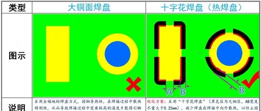
Copper pouring is an important aspect of Jialichuang’s high-density PCB design. The significance of copper pouring lies in reducing ground line impedance, enhancing anti-interference capability; lowering voltage drop, improving power efficiency; and connecting with the ground line to reduce loop area. It is advisable to use cross pads on copper pouring surfaces We know that … Read more
How to Design Efficient and Aesthetic PCB Layouts

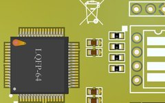
How to Design Efficient and Aesthetic PCB Layouts

1. PCB Layout 1. Follow the layout principle of “big first, small later, difficult first, easy later”, meaning that important unit circuits and core components should be prioritized in the layout. 2. The layout must refer to the schematic diagram and place components according to the signal flow rules of the schematic. 3. The arrangement … Read more