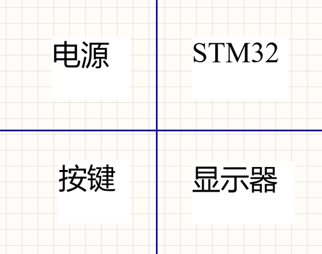
1. PCB Layout
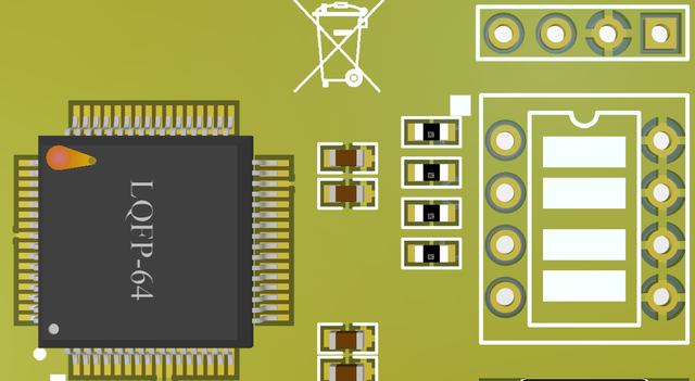
1. Follow the layout principle of “big first, small later, difficult first, easy later”, meaning that important unit circuits and core components should be prioritized in the layout.
2. The layout must refer to the schematic diagram and place components according to the signal flow rules of the schematic.
3. The arrangement of components should facilitate later debugging and maintenance, with sufficient space around components that need debugging.
4. Heating components should be evenly distributed to enhance the heat dissipation of both the single board and the entire machine, and all temperature-sensitive devices, except temperature detection components, should be kept as far away as possible from high-heat components.
5. The layout should meet the following requirements as much as possible: the shortest total connections and shorter critical signal lines; complete separation of high-voltage signals from low-voltage weak signals; separation of analog signals from digital signals; separation of high-frequency signals from low-frequency signals; and sufficient spacing for high-frequency components.
6. During component layout, consider grouping components that use the same power supply together.
2. Wiring
Prioritize Key Signal Lines: Key signals such as analog signals, high-speed signals, clock signals, and synchronous signals should be prioritized in wiring.
Provide dedicated wiring layers for clock signals, high-frequency signals, and sensitive signals, ensuring the smallest loop area.
Density Priority Principle: Start wiring from the components with the most complex connections and the densest areas on the board.
Networks with impedance control requirements should be wired according to the line length and width requirements as much as possible.
Wiring Methods:
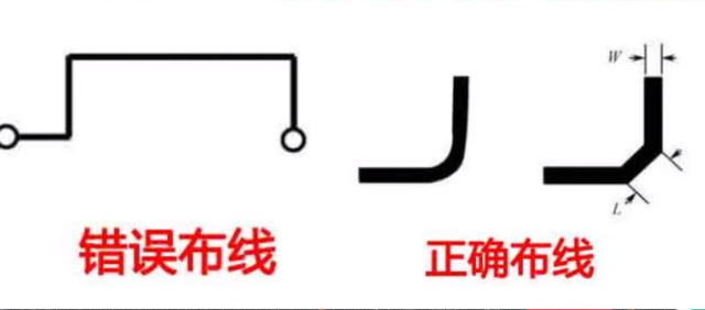
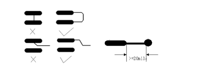
1. Right-Angle Wiring:
Right-angle wiring causes the copper foil at the corners to be 1.414 times the normal line width, resulting in a sudden change in characteristic impedance at the right-angle bends. This has little impact on ordinary wiring, but for high-speed signals, changes in characteristic impedance can lead to signal reflections, degrading signal quality. Additionally, the extra parasitic capacitance at the corners can cause delay in signal transmission. Moreover, right-angle tips are prone to emit or receive electromagnetic waves, resulting in EMI issues.
2. Short Lines and Loops
During design, keep wiring lengths as short as possible to reduce interference caused by long traces, especially for important signal lines like clock lines, ensuring that the oscillator is placed close to the device. The main goal is to adjust the delay to meet the system’s timing requirements.
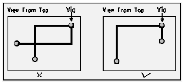
Prevent signal lines from forming self-loops between different layers. This issue is common in multilayer board designs, and loops can cause radiated interference.
3. S-shaped Lines
S-shaped lines are a commonly used wiring method in PCBs. Their main purpose is to adjust the delay to satisfy the system’s timing requirements. However, S-shaped routing can degrade signal quality and alter transmission delays, so it should be avoided when possible. In practice, signal lines often need to be routed this way to minimize timing offsets between signals in the same group, leading to intentional routing. Generally, parallel routing should be employed, minimizing vias; when vias are necessary, they should be done in pairs to achieve impedance matching. Groups of buses with similar attributes should be routed side by side to maintain equal lengths. Vias leading from surface mount pads should be kept as far from the pads as possible.
3. Copper Pouring
Whether for power or signal, there is always a return path. No matter where the current flows, it must return. Therefore, in our circuits, any signal exists in the form of a closed loop. Our power ground refers to the path of current in the power circuit, which usually carries a large current, while our signal ground is primarily the return path for our device module signals. Thus, we can use copper pouring to reduce wiring and increase ground area, achieving ground integrity.
Source: Internet