A good circuit board not only needs to achieve the functionality of the circuit design but also must consider electrical characteristics such as EMI, EMC, ESD (Electrostatic Discharge), and signal integrity. Additionally, mechanical structure and heat dissipation issues for high-power chips must be taken into account. On this basis, the aesthetic aspect of the circuit board should also be considered, akin to artistic sculpture, where every detail is carefully deliberated.
Common PCB Layout Constraint Principles often involve the following considerations when laying out PCB components:
- Does the PCB shape match the overall device?
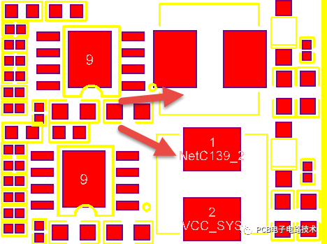
- Is the spacing between components reasonable? Are there any conflicts in height or horizontal alignment?
- Does the PCB require panelization? Are there reserved process edges? Are there reserved mounting holes? How should positioning holes be arranged?
- How should the power module be placed and how is heat dissipation managed?
- Is the placement of frequently replaced components convenient for replacement? Are adjustable components easy to adjust?
- Is the distance between heat-sensitive components and heat-generating components considered?
- What is the overall EMC performance of the board? How can the layout effectively enhance anti-interference capability?
Regarding the spacing issue between components, different packaging types have varying distance requirements, and due to the characteristics of Altium Designer, if constraints are set through rules, it can become overly complex and difficult to implement. Generally, mechanical layers are used to draw lines indicating the outer dimensions of components, as shown in Figure 9-1, so that when other components approach, the spacing can be roughly estimated. This is very practical for beginners and helps them develop good PCB design habits.
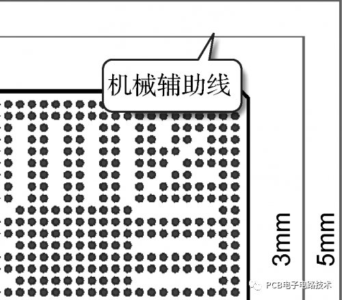
Figure 9-1 Mechanical Auxiliary Lines
Based on the above considerations, the common PCB layout constraint principles can be classified as follows:
Component Arrangement Principles
- Under normal conditions, all components should be arranged on the same side of the PCB. Only when the top layer components are too dense can some low-profile and low-heat-generating components (such as surface mount resistors, capacitors, ICs, etc.) be placed on the bottom layer.
- To ensure electrical performance, components should be placed on a grid and arranged parallel or perpendicular to each other for neatness and aesthetics. Generally, overlapping components is not allowed, and the arrangement should be compact, with input and output components kept as far apart as possible to avoid crossing.
- For components or wires that may have high voltage, increase their distance to prevent accidental short circuits due to discharge or breakdown. Pay attention to the layout space for these signals.
- High-voltage components should be placed in locations that are difficult to reach during debugging.
- Components located at the edge of the board should be at least two board thicknesses away from the edge.
- Components should be evenly distributed across the board surface, avoiding dense areas in one region and sparse areas in another to improve product reliability.
Layout Principles According to Signal Direction
- After placing fixed components, arrange the positions of each functional circuit unit according to the flow of signals, centering around the core components of each functional circuit for local layout.
- The layout of components should facilitate signal flow, keeping the signal direction as consistent as possible. In most cases, the signal flow is arranged from left to right or from top to bottom, with components directly connected to input and output terminals placed close to the input/output connectors.
Preventing Electromagnetic Interference
- For components that radiate strong electromagnetic fields and those sensitive to electromagnetic induction, increase the distance between them or consider adding shielding covers.
- Avoid mixing high and low voltage components and interleaving strong and weak signal components.
- For components that generate magnetic fields, such as transformers, speakers, and inductors, the layout should minimize the cutting of magnetic field lines on printed conductors. The magnetic field directions of adjacent components should be perpendicular to reduce mutual coupling. Figure 9-2 shows inductors arranged at a 90° angle.
- Shield interference sources or modules that are easily disturbed, ensuring that the shielding cover has good grounding. The planning of the shielding cover is shown in Figure 9-3.
Suppressing Thermal Interference
- For heat-generating components, prioritize their arrangement in locations conducive to heat dissipation. If necessary, separate heat sinks or small fans can be set up to lower temperatures and reduce the impact on adjacent components, as shown in Figure 9-4.
- High-power integrated circuits, high-power transistors, resistors, etc., should be arranged in places that facilitate heat dissipation and kept at a certain distance from other components.
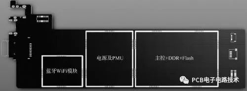
Figure 9-3 Planning of Shielding Covers
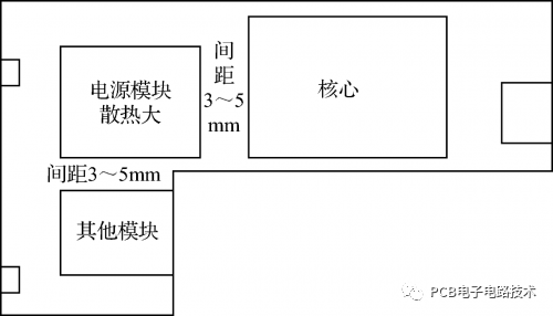
Figure 9-4 Considerations for Layout Heat Dissipation
- Heat-sensitive components should be placed close to the components being measured and away from high-temperature areas to avoid being affected by other heat-generating components, which could cause erroneous actions.
- When placing components on both sides, generally, do not place heat-generating components on the bottom layer.
Adjustable Component Layout Principles
For adjustable components such as potentiometers, variable capacitors, adjustable inductors, and micro switches, the layout should consider the structural requirements of the entire device: if it is externally adjustable, its position should correspond to the position of the adjustment knob on the chassis panel; if it is internally adjustable, it should be placed on the PCB in a location that is convenient for adjustment.


Source: Network
Copyright Notice: The copyright of the above text and images belongs to the original author. The “Meizhou Printed Circuit Industry Association” shares this as a reprint. If there are any copyright issues, please contact us for removal.