
In integrated circuit application design, after completing the project schematic design, the next step is to design the PCB layout.PCB design is a crucial step.The quality of the design results directly affects the overall functionality of the design.Therefore, a reasonable and efficient PCB Layout is a critical step in the successful debugging of chip circuit design.In this article, we will briefly discuss the key points of PCB Layout design.
Key Points of PCB Layout Design
Component Package Selection
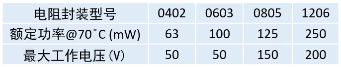
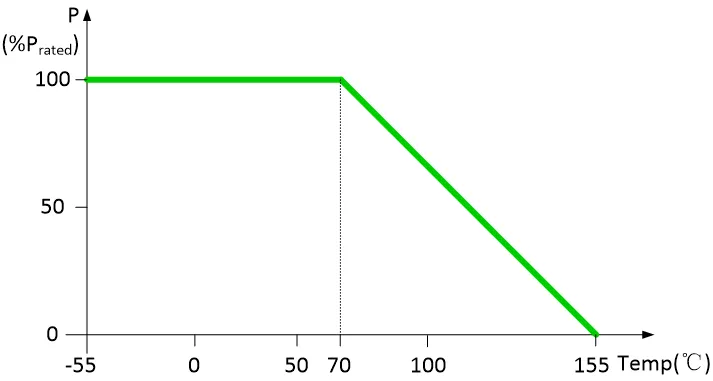
Resistor Selection: The selected resistor’s voltage rating, maximum power, and temperature must not exceed the operating range.
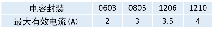
Capacitor Selection: When selecting, it is also necessary to consider the voltage rating and maximum effective current of the chosen capacitor.
Inductor Selection: The selected inductor’s effective current and peak current must be greater than the actual current flowing through the circuit.
Common Interference in Circuit Design
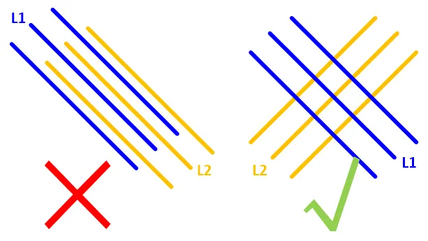
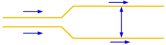
Crosstalk: When the parallel routing distance of the design lines is too long, the mutual capacitance and mutual inductance between the conductors can couple energy to adjacent transmission lines. Crosstalk can be reduced by the following methods:
1. Add safety routing

2. Try to make adjacent lines perpendicular to each other
3. Increase the spacing between parallel lines for every distance traveled
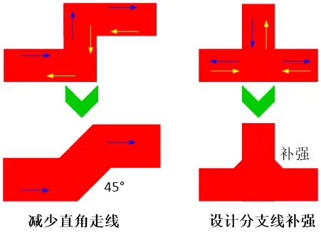
Reflection: Due to the corners and excessive branches in the wiring, impedance mismatches can occur on the transmission line. This can be improved by reducing the corners and branches in the lines or avoiding right-angle wiring and branch line reinforcements.
Determine Grounding Method
Single Point Grounding (suitable for low-frequency circuits): All circuit ground wires connect to a common ground point, simplifying connections and reducing interference from ground loops.
Multi-Point Grounding (suitable for multilayer circuit/high-frequency circuits): Each part of the system is grounded nearby, providing lower ground impedance.
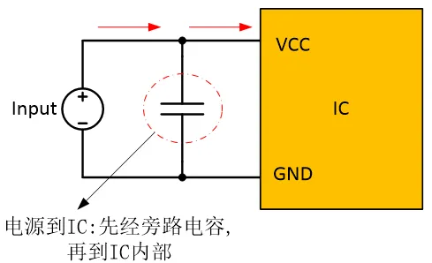
Add Filtering and Bypass Capacitors
To ensure stable input/output voltage, add input/output capacitors.
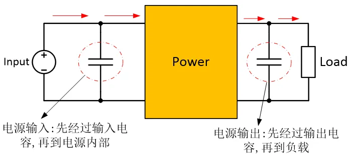
Add bypass capacitors between the power supply and IC to ensure stable input voltage and filter out high-frequency noise.
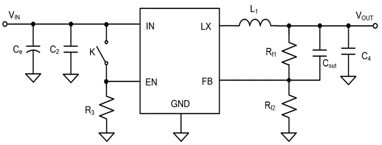
Impedance Position Design

Generally, the higher the impedance position, the more susceptible it is to interference. Below is the PCB impedance position design for a synchronous buck chip.
PCB Layout Design Techniques
Power/Ground Line Handling
Even if the wiring throughout the PCB is well done, interference caused by inadequate consideration of power and ground lines can degrade product performance. When routing, try to widen the power and ground line widths; ideally, the ground line should be wider than the power line. Their relationship is: ground line > power line > signal line.
For digital circuit PCBs, a wide ground conductor can form a loop, effectively creating a ground network (this method cannot be used for analog circuits). Use large copper areas as ground, connecting all unused areas of the printed board to ground. Alternatively, use multilayer boards, with power and ground lines occupying one layer each.
Common Ground Handling for Digital and Analog Circuits
When digital and analog circuits coexist, wiring must consider mutual interference, especially noise interference on the ground line.
Digital circuits operate at high frequencies, while analog circuits are highly sensitive. For signal lines, high-frequency signal lines should be kept as far away as possible from sensitive analog circuit components.
For ground lines, the entire PCB has only one external connection port, so the common ground issue between digital and analog must be handled internally. Internally, the digital ground and analog ground are actually separated and not connected to each other, only at the external connection port (such as a connector), the digital ground and analog ground have a slight short connection. Please note, there is only one connection point.
Signal Line Distribution Layer
Signal lines are placed on the power (ground) layer: In multilayer printed boards, if there are few remaining lines on the signal line layer, adding more layers will cause waste and increase production workload, thus increasing costs.
To resolve this conflict, consider routing on the power (ground) layer. First, consider using the power layer, and then the ground layer, as it is best to maintain the integrity of the ground layer.
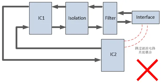
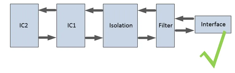
Signal Flow Direction Design
During PCB layout design, the principle of placing components in a straight line along the signal flow direction should be fully adhered to, avoiding back-and-forth routing as much as possible.
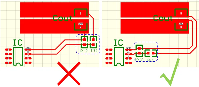
PCB Layout Design Examples
Layout Design Recommendations
1. Place the driver chip as close as possible to the power MOSFET;
2. Place the VCC-GND (CVCC) / VB-VS (CBS) capacitors as close as possible to the chip;
3. Add a certain number of vias to the chip’s heat dissipation pad and connect it to GND (to increase heat dissipation and reduce parasitic inductance);
4. Connect the GND wiring directly to the source of the MOSFET, avoiding overlap with the high current path between source and drain, and apply the same principle to VS GND wiring (avoid overlapping power and drive circuits);
5. Make the HO/LO wiring as wide as possible (60mil-100mil, as the driving current is relatively high, to reduce the impact of parasitic inductance);
6. Keep the LIN/HIN logic input ports as far away as possible from HS wiring (to avoid high voltage swings interfering with input signals).
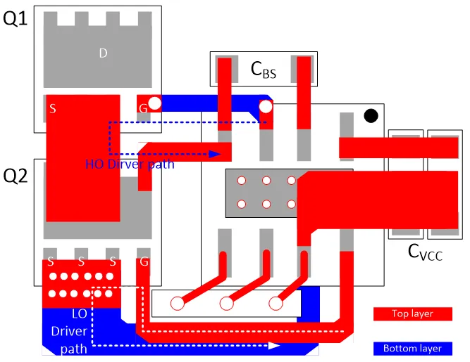
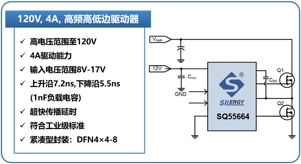
*SQ55664 Layout Design
Source: Internet