Jialichuang Plans IPO: Launch of 34 to 64-Layer Ultra-High-Density PCBs and HDI Products, Accelerating High-End Strategy?
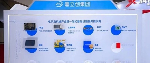
As the global electronics industry evolves towards high performance and miniaturization, printed circuit boards (PCBs), as core foundational components, are becoming crucial for hardware innovation. Jialichuang Group (hereinafter referred to as “Jialichuang”), a one-stop electronic and mechanical industry chain service provider that started with PCB prototyping, recently announced the mass production of 34 to 64-layer … Read more