1. Problem Description A certain dashcam requires an external adapter for testing. During power-on testing, it was found to exceed standards, specifically at frequencies of 84MHz, 144MHz, and 168MHz. The cause of the excessive radiation needs to be analyzed, and corresponding countermeasures should be provided. The radiation test data is as follows: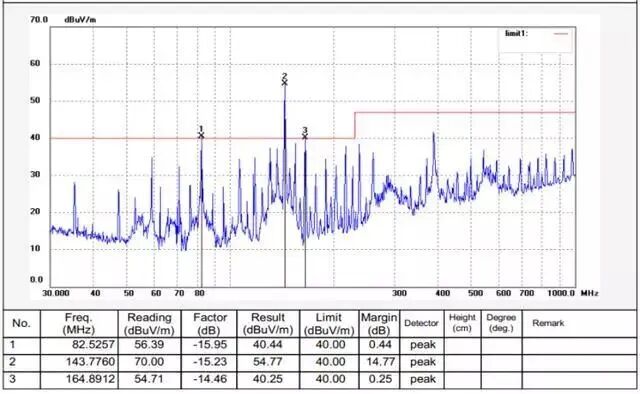 2. Analysis of Radiation Sources This product has only one PCB, which contains a 12MHz crystal. The frequencies that exceed standards are all multiples of 12MHz. Analyzing the machine’s EMI radiation, the LCD-CLK is found to be 33MHz, while the camera MCLK is 24MHz. Upon exclusion, it was found that removing the camera still resulted in exceeding standards. However, shielding the 12MHz crystal reduced the excessive points, indicating that the 144MHz excess is related to the crystal. The PCB layout is as follows:
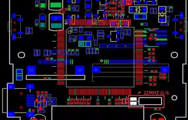 3. Principles of Radiation Generation From the PCB layout, it can be seen that the 12MHz crystal is positioned right at the edge of the PCB. When the product is placed in a radiation emission testing environment, the high-speed components of the tested product and the reference ground in the laboratory form a certain capacitive coupling, generating parasitic capacitance, which leads to common-mode radiation. The larger the parasitic capacitance, the stronger the common-mode radiation. The parasitic capacitance is essentially the electric field distribution between the crystal and the reference ground. When the voltage between the two is constant, the more electric field distribution there is between them, the greater the electric field strength, and the larger the parasitic capacitance. The electric field distribution of the crystal at the edge of the PCB compared to that in the middle of the PCB is as follows:
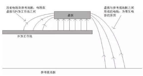 Schematic diagram of the electric field distribution between the crystal at the PCB edge and the reference ground plane
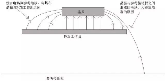 Schematic diagram of the electric field distribution between the crystal in the middle of the PCB and the reference ground plane From the diagram, it can be seen that when the crystal is placed in the middle of the PCB or further away from the edge, the presence of the ground plane (GND) in the PCB confines most of the electric field between the crystal and the working ground, i.e., inside the PCB, significantly reducing the electric field distributed to the reference ground plane, thus lowering radiation emissions.4. Countermeasures Move the crystal inward, ensuring it is at least 1cm away from the PCB edge, and apply copper on the PCB surface within 1cm of the crystal. Additionally, connect the surface copper to the PCB ground plane through vias. The spectrum diagram of the test results after modification is as follows, showing a significant improvement in radiation emissions.
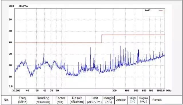 5. Reflections and Insights The capacitive coupling between high-speed printed lines or components and the reference ground plane can lead to EMI issues. Sensitive printed lines or components placed at the edge of the PCB can create susceptibility problems. If the design necessitates placement at the PCB edge for other reasons, a working ground line can be laid alongside the printed line, and additional vias can be added to connect this working ground line to the working ground plane.

Disclaimer: This article is original by the author, and the content reflects the author’s personal views. The Electronics Enthusiast Network reproduces it only to convey a different perspective and does not represent the endorsement or support of this viewpoint by the Electronics Enthusiast Network. If there are any objections, please contact the Electronics Enthusiast Network. More Exciting Articles to Read
-
Low accuracy of infrared thermometers, whose fault is it? Sensor, MCU, algorithm, or detection?
-
Memory prices will rise quarter by quarter in 2020, is it just due to the pandemic?
-
How to view the impact of “new infrastructure” on China’s semiconductor industry?
-
Nearly 60% of companies have resumed work, and 70% of companies are under financial strain – a deep scan of the impact of the COVID-19 pandemic on the electronic supply chain.
-
Temperature measuring helmets are gaining momentum, accelerating deployment under the pandemic.