Comprehensive Analysis of PCB Layout Design Key Points

Comprehensive Analysis of PCB Layout Design Key Points

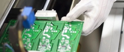
▲ Click the blue text above to follow us and never miss any valuable articles! In electronic circuit systems, printed circuit boards (PCBs) are the key carriers for mounting electronic components and achieving electrical connections. The PCB Layout design is the core aspect that determines the performance of the PCB. From the signal integrity of … Read more
PCB Without Mark Points: The Critical SMT ‘Lifeline’ Engineers Must Be Aware Of

PCB Without Mark Points: The Critical SMT 'Lifeline' Engineers Must Be Aware Of

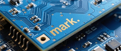
In microcontroller development, we often need to hand over the designed PCB files to the factory for production. Recently, one of our engineers encountered a troubling issue, as the PCB board lacked Mark points, resulting in deductions from the SMT factory. Today, we will discuss this topic: how important are Mark points in SMT processing? … Read more

PCB Molding and Design Relationship

PCB Molding and Design Relationship

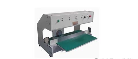
The design of PCBs is closely related to the production and subsequent use of PCBs and PCBA. This article introduces the relationship between PCB molding, panel separation, and PCB design.01 Introduction to Molding and Panel Separation MethodsThe working panel is molded into a shipping panel, which is generally done using a board retrieval machine; the … Read more

Requirements and Considerations for PCB Silkscreen Design

Requirements and Considerations for PCB Silkscreen Design

Silkscreen design is an essential factor in PCB design. The silkscreen on a PCB typically includes: component silkscreen and designators, board name, version number, anti-static symbols, barcode silkscreen, company logo, and other identifiers. Next, let’s take a look at the requirements for silkscreen design in PCB design. 1. Silkscreen Design Requirements The height-to-width ratio of … Read more

Design Considerations for PCB Process Edges

Design Considerations for PCB Process Edges

When performing SMT (Surface Mount Technology) processing on PCBs, the PCBs are conveyed along the SMT production line via guide rails. Therefore, a pair of edges must be reserved as forbidden areas for component placement. Typically, the two long edges of the PCB or the assembled panel are designated as the conveyance edges. The width … Read more

Composition, Design, Process, Workflow, and Principles of Component Placement and Routing for PCB Circuit Boards

Composition, Design, Process, Workflow, and Principles of Component Placement and Routing for PCB Circuit Boards

Let’s learn about the composition, design, process, workflow, and principles of component placement and routing for PCB circuit boards, along with some considerations for the later stages! Composition of PCB Circuit Boards 1. Lines and Planes: The lines serve as the conductive paths between components, and a large copper area is designed separately for grounding … Read more