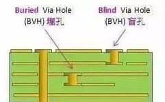
General Principles of PCB Layout and Wiring in AD
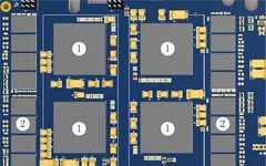
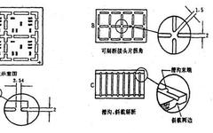
1 Layout Principles 1. Follow the layout principle of “large first, small later; difficult first, easy later,” meaning that important circuit units and core components should be prioritized in layout. Large first, small later; difficult first, easy later In the above image, 1 is positioned due to mechanical structure determining the power supply and terminal … Read more