The process of transforming a printed circuit board from a blank panel to revealing the circuit patterns is a complex series of physical and chemical reactions. This article will analyze the final step—etching.
Currently, the typical processing method for printed circuit boards (PCBs) employs the “pattern plating method”. This means that a lead-tin resist layer is first plated on the copper foil portion of the board that needs to be retained, which is the part of the circuit pattern, and then the remaining copper foil is chemically corroded away, known as etching.
Types of Etching
It is important to note that there are two layers of copper on the board during etching. In the outer layer etching process, only one layer of copper must be completely etched away, while the rest will form the final required circuit. This type of pattern plating is characterized by the copper layer existing only beneath the lead-tin resist layer.
Another method involves plating copper over the entire board, with the areas outside the photosensitive film only being covered by a tin or lead-tin resist layer. This method is referred to as the “full board copper plating process”. Compared to pattern plating, the biggest disadvantage of full board copper plating is that copper must be plated twice across the board surface, and during etching, all of it must be corroded away. Therefore, when the wire width is very fine, a series of problems may arise. Additionally, side etching can severely affect the uniformity of the lines.
In the processing of the outer circuit of the printed board, there is another method that uses a photosensitive film instead of a metal plating layer as the resist layer. This method is very similar to the inner layer etching process; refer to the etching in the inner layer manufacturing process.
Currently, tin or lead-tin is the most commonly used resist layer, applied in the etching process with ammonia-based etchants. Ammonia-based etchants are widely used chemical solutions that do not react chemically with tin or lead-tin. Ammonia-based etchants primarily refer to ammonia/chloride etching solutions.
Additionally, ammonia/sulfuric ammonium etching solutions can also be purchased on the market. Etching solutions based on sulfates can be reused as the copper within can be separated by electrolysis after use. Due to its low corrosion rate, it is generally not seen in actual production, but it is expected to be used in chlorine-free etching.
Some have experimented with sulfuric acid-hydrogen peroxide as an etching agent to corrode the outer pattern. For many reasons, including economic and waste treatment aspects, this process has not been widely adopted commercially. Furthermore, sulfuric acid-hydrogen peroxide cannot be used for etching lead-tin resist layers, and this method is not a primary method in PCB outer layer production, so very few people inquire about it.
Etching Quality and Existing Issues
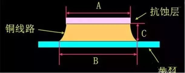
The basic requirement for etching quality is to completely remove all copper layers except for those beneath the resist layer, and that is all. Strictly speaking, if precisely defined, etching quality must include the consistency of wire width and the degree of side etching. Due to the inherent characteristics of the etching solution, etching occurs not only downward but also in lateral directions, making side etching almost unavoidable.
Side etching is a frequently discussed topic in etching parameters, defined as the ratio of side etching width to etching depth, known as the etching factor. In the printed circuit industry, its variation range is quite broad, from 1:1 to 1:5. Clearly, a small side etching degree or low etching factor is the most desirable.
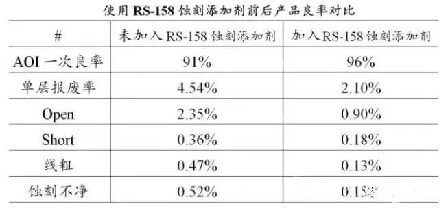
The structure of the etching equipment and the different components of the etching solution can affect the etching factor or side etching degree. Optimistically speaking, it can be controlled. Using certain additives can reduce side etching. The chemical composition of these additives is generally a trade secret, and their developers do not disclose it to the public.
In many respects, the quality of etching is determined before the printed board enters the etching machine. This is because there are very tight internal connections between the various processes or operations in printed circuit processing. No operation is unaffected by others. Many issues identified as etching quality problems actually existed in earlier processes, even before the film removal.
For the outer pattern etching process, because it exhibits the “inverse stream” phenomenon more prominently than most printed board processes, many problems ultimately reflect on it. Additionally, this is due to etching being the last link in a long series of processes, starting with the self-adhesive film and culminating in the successful transfer of the outer pattern. The more links there are, the greater the possibility of problems arising. This can be seen as a very unique aspect of the printed circuit production process.
In theory, once the printed circuit enters the etching stage in the pattern plating method for processing printed circuits, the ideal state should be that the total thickness of the plated copper and tin or copper and lead-tin does not exceed the thickness of the resist film that can withstand plating, completely blocking the plated pattern with the “walls” on both sides and embedding it. However, in actual production, the plated patterns on printed circuit boards worldwide after plating are generally much thicker than the photosensitive patterns. During the plating of copper and lead-tin, due to the height of the plated layer exceeding the photosensitive film, there is a tendency for lateral accumulation, leading to problems. The lead or lead-tin resist layer covering over the lines extends to both sides, forming “ledges” that cover a small part of the photosensitive film below the “ledge”.
The “ledge” formed by the tin or lead-tin makes it impossible to completely remove the photosensitive film during film removal, leaving a small amount of “residue” beneath the “ledge”. The “residue” or “remaining film” left beneath the resist “ledge” will cause incomplete etching. After etching, “copper roots” form on both sides of the lines, causing the spacing between lines to narrow, resulting in the printed board not meeting the client’s requirements and potentially being rejected. Due to rejections, the production cost of PCBs will significantly increase.
Furthermore, in many cases, due to reactions that cause dissolution, residues and copper may also accumulate in the etching solution in the printed circuit industry, clogging the nozzles of the etching machine and acid-resistant pumps, necessitating stopping to handle and clean, which affects work efficiency.
Equipment Adjustment and Interaction with Etching Solutions
In printed circuit processing, ammonia etching is a relatively fine and complex chemical reaction process. Conversely, it is also an easy task to perform. Once the process is adjusted, production can continue uninterrupted. The key is to maintain a continuous working state once the machine is started; it should not be intermittent. The etching process greatly relies on the good working condition of the equipment. Currently, regardless of the etching solution used, high-pressure spraying must be employed, and to achieve neat line edges and high-quality etching results, the structure and spraying method of the nozzles must be strictly selected.
To achieve good side effects, many different theories have emerged, forming various design methods and equipment structures. These theories are often vastly different. However, all theories related to etching acknowledge one fundamental principle: to allow the metal surface to continuously contact fresh etching solution as quickly as possible. The chemical mechanism analysis of the etching process also confirms this viewpoint. In ammonia etching, assuming all other parameters remain unchanged, the etching rate is primarily determined by the ammonia (NH3) in the etching solution. Therefore, the purpose of allowing fresh solution to interact with the etching surface is twofold: to wash away the copper ions just produced and to continuously provide the ammonia (NH3) needed for the reaction.
In the traditional knowledge of the printed circuit industry, especially among suppliers of printed circuit materials, it is widely recognized that the lower the content of monovalent copper ions in ammonia etching solutions, the faster the reaction speed. This has been confirmed by experience. In fact, many ammonia etching solution products contain special ligands for monovalent copper ions (some complex solvents), which serve to reduce monovalent copper ions (this is the technical secret that gives their products high reactivity). It is evident that the influence of monovalent copper ions is significant. Reducing monovalent copper from 5000ppm to 50ppm can more than double the etching rate.
Due to the generation of a large number of monovalent copper ions during the etching reaction process, and since monovalent copper ions are always tightly bound to ammonia’s ligands, maintaining their content close to zero is very difficult. The conversion of monovalent copper to divalent copper can be achieved through the action of oxygen in the atmosphere, allowing for the removal of monovalent copper. This can be achieved by spraying.
This is one of the functional reasons for introducing air into the etching tank. However, if there is too much air, it will accelerate the loss of ammonia in the solution, causing the pH to drop, which will ultimately reduce the etching rate. The variation of ammonia in the solution also needs to be controlled. Some users adopt the practice of introducing pure ammonia into the etching storage tank. This requires an additional pH meter control system. When the automatically measured pH result falls below a specified value, the solution will automatically be replenished.
In the related field of chemical etching (also known as photochemical etching or PCH), research work has begun and has reached the stage of etching machine structure design. In this method, the solution used is divalent copper, not ammonia-copper etching. It may be used in the printed circuit industry. In the PCH industry, the typical thickness of etched copper foil is 5 to 10 mils, and in some cases, the thickness is quite large. Its requirements for etching parameters are often more stringent than those in the PCB industry.
Different Issues Regarding Etching States
A large number of issues related to etching quality are concentrated on the parts of the board surface that are being etched. It is very important to understand this. These problems arise from the influence of gelled residues produced by the etching agent on the upper surface of the printed circuit board. Gelled residues accumulate on the copper surface, affecting the jet force on one hand and blocking the replenishment of fresh etching solution on the other, resulting in a decrease in etching speed. It is precisely due to the formation and accumulation of gelled residues that the etching degree of the upper and lower patterns of the board differs. This also causes the part of the board that enters the etching machine first to be etched thoroughly or easily over-etched, as the accumulation has not yet formed, resulting in a faster etching speed. Conversely, the part of the board that enters later has already formed accumulation, slowing its etching speed.
Maintenance of Etching Equipment
The key factor in the maintenance of etching equipment is to ensure the cleanliness of the nozzles, free from blockages to allow smooth spraying. Blockages or residues can strike the surface under the pressure of spraying. If the nozzles are unclean, it can lead to uneven etching, rendering the entire PCB scrap.
Maintenance of the equipment involves replacing damaged and worn parts, including replacing nozzles, which also face wear issues. Additionally, a more critical issue is to ensure that the etching machine does not have residue accumulation, which occurs frequently. Excessive accumulation can even affect the chemical balance of the etching solution. Similarly, if the etching solution exhibits excessive chemical imbalance, the residue accumulation will become more severe. The issue of residue accumulation cannot be overstated. Once the etching solution suddenly shows a significant amount of residue, it is usually a signal that the balance of the solution has problems. This should be cleaned appropriately with strong hydrochloric acid or replenished into the solution.
Residues can also produce solid residues; a small amount of residues dissolve in the etching solution and then form copper salt precipitates. The residues formed indicate that the previous film removal process was not thorough. Poor film removal is often the result of edge film and over-plating.
Note: The copyright of this article belongs to the original author and does not represent the views of the association. The articles promoted by the “Jiangxi Provincial Electronic Circuit Industry Association” are for sharing purposes only and do not represent the position of this account. If there are copyright issues, please contact us for removal.