12 Details for PCB Layout
12 Details for PCB Layout

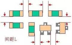
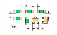
1. Spacing Between SMDs The spacing between SMDs should neither be too large (which wastes PCB area) nor too small to avoid solder paste printing adhesion and difficulties in soldering repairs. The spacing can refer to the following specifications: ■ Same component: ≥ 0.3mm■ Different components: ≥ 0.13×h+0.3mm (h is the maximum height difference between … Read more
General Principles of PCB Layout and Wiring in AD

General Principles of PCB Layout and Wiring in AD

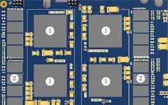
1 Layout Principles 1. Follow the layout principle of “large first, small later; difficult first, easy later,” meaning that important circuit units and core components should be prioritized in layout. Large first, small later; difficult first, easy later In the above image, 1 is positioned due to mechanical structure determining the power supply and terminal … Read more

10 PCB Layout Details You Might Not Know!

10 PCB Layout Details You Might Not Know!

PCB Layout is a meticulous task that involves not only regulatory constraints but also numerous details that engineers need to consider. In this article, we have compiled some critical details to pay attention to in layout design. Let’s see if you are aware of them! 1. Layout of Special Components √ Heat-generating components should be … Read more

12 Important Details to Consider in PCB Layout

12 Important Details to Consider in PCB Layout

1. Spacing Between SMD Components The spacing between SMD components is a crucial issue that engineers must pay attention to during layout. If the spacing is too small, it becomes very difficult to print solder paste and avoid solder bridging.The recommended distances are as follows: Spacing requirements for SMD components: Same type of components:≥0.3mm Different … Read more

How to Design a Perfect PCB

How to Design a Perfect PCB

1. Layout 10 Rules for Component Layout: 1. Follow the principle of “large first, small later, difficult first, easy later,” meaning important circuit units and core components should be laid out first. 2. The layout should refer to the schematic diagram, arranging major components based on the main signal flow direction of the board. 3. … Read more

PCB Layout Tips and Considerations

PCB Layout Tips and Considerations

There are many factors that engineers need to consider. This article organizes some detailed issues that need attention in PCB layout. Let’s check if you are aware of them! 01 Layout of Special Components Heating components should be placed in a location conducive to heat dissipation, such as the edge of the PCB, and away … Read more

Checklist Before IC Tape-Out

Checklist Before IC Tape-Out

Click to View: Christmas Benefits | Free 3-Month VIP Membership for E-Course Network! Abstract: Before tape-out, it is necessary to check the layout, routing, drive/load, IO, and design rules of the chip. Based on years of tape-out experience, the necessary checks for each part are summarized as follows. 1. Layout Check 1) Consider the direction … Read more