 Click the blue words above to follow PCB knowledge
Many newcomers to PCB design think that once they finish the PCB design, they can go home. No, no, no, that’s not the case. When the PCB files are sent to the manufacturing factory, various problems often arise during the PCB processing, such as solder bridging after wave soldering. Although it may not necessarily be the fault of the PCB design, it’s better to be safe than sorry. If you truly become the scapegoat, it could lead to serious issues!
So today, we are going to refuse to be the scapegoat and strive to reduce errors in PCB design, starting with wave soldering!
 What is wave soldering?
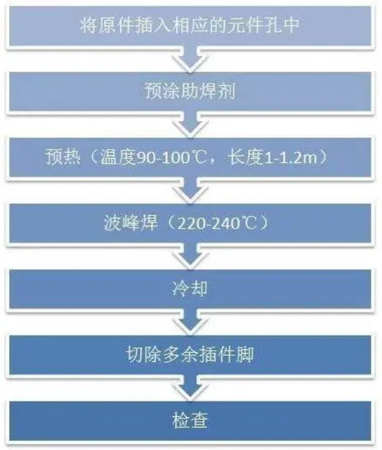
Wave soldering refers to the process where the soldering surface of the plug-in board directly contacts high-temperature liquid solder to achieve soldering. During this process, the high-temperature liquid solder maintains an inclined surface, creating a wave-like phenomenon through special devices. The main material used is solder bars, as shown in the figure, which illustrates the wave soldering formation process.
What is solder bridging?
According to IPC-A-610D, when two or more solder joints are connected by solder, resulting in defects in appearance and function on the PCB, it is referred to as solder bridging.
Causes of solder bridging on PCBs after wave soldering
First, it is important to understand that the occurrence of solder bridging on a PCB is not necessarily the fault of the PCB design. It could also be due to various factors during wave soldering, such as poor flux activity, insufficient wettability, uneven application, and improper control of preheating and solder temperatures.
Once it is determined that the problem lies with the PCB design, we can consider the following factors:
① Is the transmission direction of the plug-in correct?
② Is the initial board length of the plug-in pins too long?
③ Is the distance between solder joints of wave soldering components appropriate?
④ If the spacing does not meet process requirements, have solder pads and silk screen ink been added?
How to avoid solder bridging in PCB design?
1. Choose appropriate components
If the PCB is to be wave soldered, it is recommended that the spacing between the selected components (the center-to-center distance between pins) be ≥ 2.54mm, and at least greater than 2.0mm. Otherwise, there will be a risk of solder bridging. It is also advisable to appropriately modify and optimize the pads to meet processing requirements and avoid solder bridging.
2. Green oil bridges must be no less than 2 mil
The green oil bridge must be no less than 2 mil (except for surface-mounted components with dense pins like QFP packages), otherwise, it may easily lead to solder bridging during processing.
3. Add solder pads
Adding solder pads can reduce the probability of solder bridging. Depending on the layout requirements of the components on the PCB, add solder pads at the end of the transmission direction. The size of the solder pads can be adjusted based on the density of the PCB.
4. Drag soldering pieces
If the PCB needs to use components with dense spacing, install drag soldering pieces at the tin position of the fixture to prevent solder paste from clumping and causing solder bridging on the component pins.
5. Solder pin spacing
When the solder pins on the PCB protrude more than 2mm, it is easy to cause solder bridging. Therefore, as long as the length of the pins protruding from the board is ≤ 1mm, the probability of solder bridging for dense pin components will be greatly reduced.
6. Direction of component length relative to the PCB
The length direction of the component should be consistent with the transmission direction on the board, which will significantly reduce the number of pins that need to be addressed for solder bridging and also lower the difficulty of handling.
7. Copper ring spacing must not be less than 0.5mm
The spacing of copper rings must not be less than 0.5mm. White oil should be added between copper rings, and during PCB design, care should be taken to avoid silk screen white oil in the solder pad opening area.
The above are the techniques for avoiding solder bridging in PCB design. Have you learned them? Did they help your design in any way? If you think it’s good, feel free to share it so more people can see.
Additionally, if you have more questions, you can check out the newly launched “90-Day PCB Practical Talent Training Course by Fanyi Education”, which is specially designed for companies.
It is also a training course created by several top PCB design engineers, specifically for PCB engineers, featuring practical training and teaching to ensure companies and engineers can learn without worries, shortening the learning cycle for engineers, enhancing their project experience and technical level. Customized courses can be developed based on the company’s model and development prospects, which can also enhance the company’s competitiveness. There are many discounts for new products, so hurry up and grab them!

Registration fee: Sign up for 3 and get 1 free, sign up for 5 and get 2 free
For corporate team registrations, the lowest price is 2785/person
▼ Scan the QR code to register or inquire ▼

 Scan to add us
Contact customer service to register immediately

This article is an original piece by Fanyi Corporate Training; please indicate the source when reprinting!Submissions/Recruitment/Advertising/Course Cooperation/Resource Exchange, please add WeChat: 13237418207