Everyone knows that making a PCB board involves turning the designed schematic into a tangible PCB circuit board. Please do not underestimate this process; many things that work in theory can be difficult to implement in practice, or something that one person can achieve, another may not. Therefore, while making a PCB board is not hard, doing it well is not an easy task.
The two major challenges in the microelectronics field are handling high-frequency signals and weak signals. In this regard, the level of PCB manufacturing becomes particularly important. With the same design principles and components, different people can produce different results with their PCBs. So how can we create a good PCB board?
Based on our past experiences, I would like to discuss a few aspects:
1Clarify Design Objectives
When receiving a design task, the first step is to clarify its design objectives: whether it is a standard PCB, a high-frequency PCB, a small-signal processing PCB, or a PCB that handles both high frequency and small signals. If it is a standard PCB, it is sufficient to ensure that the layout and routing are reasonable and neat, and the mechanical dimensions are accurate. If there are medium load lines and long lines, certain measures must be taken to alleviate the load, and long lines need to be driven strongly, with a focus on preventing reflections from long lines.
When there are signal lines on the board exceeding 40MHz, special considerations must be made for these signal lines, such as crosstalk between lines. If the frequency is even higher, there are stricter limits on the length of the routing. According to the theory of distributed parameter networks, the interaction between high-speed circuits and their connections is a decisive factor that cannot be ignored during system design. As gate transmission speeds increase, opposition on signal lines will correspondingly increase, and crosstalk between adjacent signal lines will increase proportionally. Generally, the power consumption and thermal dissipation of high-speed circuits are also significant, so sufficient attention should be paid when designing high-speed PCBs.
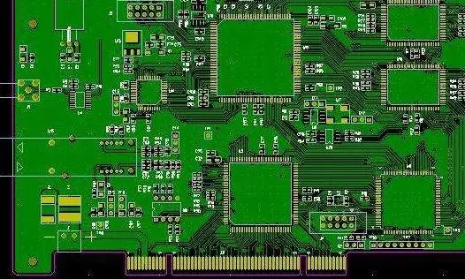 When there are millivolt-level or even microvolt-level weak signals on the board, special care must be taken for these signal lines. Weak signals are very susceptible to interference from other strong signals, so shielding measures are often necessary; otherwise, the signal-to-noise ratio will be greatly reduced, rendering useful signals submerged in noise and unable to be effectively extracted.The testing and debugging of the board should also be considered during the design stage, including the physical location of test points and isolation of test points, as some small signals and high-frequency signals cannot be measured directly with probes.Additionally, other related factors should be considered, such as the number of layers of the board, the packaging shape of the components used, and the mechanical strength of the board. Before making a PCB, one must have a clear understanding of the design objectives.
2Understand the Functional Requirements of Components for Layout and Routing
We know that some special components have specific requirements for layout and routing. For example, the analog signal amplifiers used in LOTI and APH require stable power supplies with low ripple. The analog small-signal section should be kept as far away from power devices as possible. On the OTI board, the small-signal amplification section is specially equipped with a shielding cover to block stray electromagnetic interference.
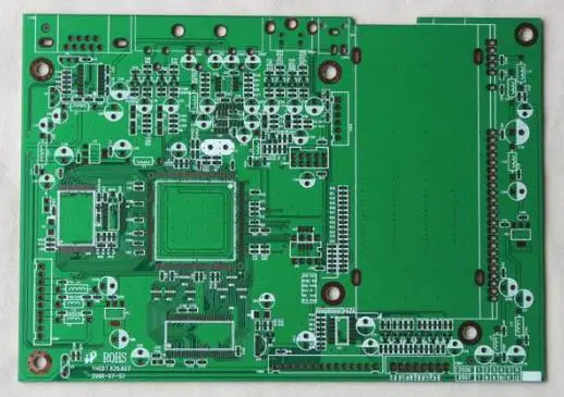
The GLINK chip used on the NTOI board adopts ECL technology, which generates significant heat due to high power consumption. Therefore, special consideration for heat dissipation must be made during layout. If natural cooling is used, the GLINK chip should be placed in a location with good airflow, and the heat dissipated should not significantly affect other chips. If the board is equipped with speakers or other high-power devices, this may cause serious power supply pollution, which should also be taken seriously.
3Considerations for Component Layout
The first factor to consider in component layout is electrical performance. Components that are closely related in connection should be placed together as much as possible, especially for high-speed lines, which should be kept as short as possible. Power signals and small-signal devices should be separated. In addition to meeting electrical performance requirements, the arrangement of components should also be neat and aesthetically pleasing, facilitating testing, and the mechanical dimensions of the board and the positions of sockets should also be carefully considered.
The grounding and transmission delay time on interconnect lines in high-speed systems are also among the primary considerations during system design. The transmission time on signal lines has a significant impact on the overall system speed, particularly for high-speed ECL circuits. Although the integrated circuit blocks themselves are fast, using ordinary interconnect lines on the baseboard (which have about 2ns of delay for every 30cm of line length) can increase delay time and significantly reduce system speed.
For synchronous components like shift registers and synchronous counters, it is best to place them on the same plug-in board, as the transmission delay time of clock signals to different plug-in boards is not equal, which could lead to errors in the shift register. If they cannot be placed on the same board, the lengths of the clock lines from the common clock source to each plug-in board must be equal at critical synchronization points.
Considerations for Routing
With the completion of the OTNI and star-shaped fiber optic network designs, there will be more boards with high-speed signal lines over 100MHz that need to be designed. Here, we will introduce some basic concepts of high-speed lines.
Transmission Lines
Any “long” signal path on a printed circuit board can be viewed as a transmission line. If the transmission delay time of that line is much shorter than the signal rise time, then the reflections produced during the signal rise will be drowned out. There will be no overshoot, undershoot, or ringing. For most MOS circuits today, because the ratio of rise time to line transmission delay time is much larger, the routing can be measured in meters without signal distortion. However, for faster logic circuits, especially ultra-fast ECL integrated circuits, due to the increase in edge speed, the length of the routing must be significantly shortened to maintain signal integrity.
There are two methods to allow high-speed circuits to operate on relatively long lines without significant waveform distortion. TTL uses Schottky diode clamping for fast falling edges, which clamps the overshoot to a level lower than ground potential by one diode drop. This reduces the undershoot amplitude. Slower rising edges allow for overshoot, but it is attenuated by the relatively high output impedance (50-80Ω) of the circuit in the “H” state. Additionally, due to the high noise immunity of the “H” state, the undershoot problem is not particularly prominent. For HCT series devices, combining Schottky diode clamping and series resistor termination will yield even better results.
When there is fan-out on signal lines, at higher bit rates and faster edge rates, the aforementioned TTL shaping methods may be insufficient. This is because reflections in the line tend to combine at high bit rates, leading to severe signal distortion and reduced noise immunity. Therefore, to address reflection issues, another method is commonly used in ECL systems: line impedance matching. This method can control reflections and ensure signal integrity.
Strictly speaking, for conventional TTL and CMOS devices with slower edge speeds, transmission lines are not always necessary. For high-speed ECL devices with faster edge speeds, transmission lines are also not always required. However, when transmission lines are used, they have the advantage of predicting line delays and controlling reflections and oscillations through impedance matching.
The basic factors that determine whether to use transmission lines are as follows:
(1) The edge speed of the system signals;
(2) The distance of the connections;
(3) Capacitive load (amount of fan-out);
(4) Resistive load (termination method for the line);
(5) Acceptable percentages of undershoot and overshoot (degree of reduction in AC noise immunity).
Types of Transmission Lines
(1) Coaxial cables and twisted pairs: These are commonly used for connections between systems. Coaxial cables typically have characteristic impedances of 50Ω and 75Ω, while twisted pairs are typically 110Ω.
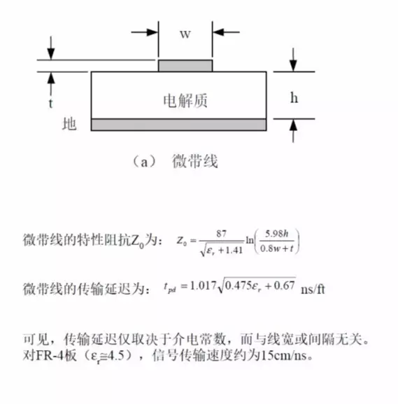
(2) Microstrip lines on printed boards
Microstrip lines are strip conductors (signal lines) isolated from the ground plane by a dielectric. If the thickness, width, and distance to the ground plane are controllable, then its characteristic impedance can also be controlled. The characteristic impedance Z0 of a microstrip line is:
(3) Strip lines in printed boards
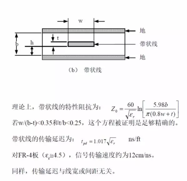
Strip lines are conductors placed between two layers of conductive planes within a dielectric. If the thickness and width of the line, the dielectric constant of the medium, and the distance between the two conductive planes are controllable, then the characteristic impedance of the strip line can also be controlled. The characteristic impedance of a strip line is:
Termination of Transmission Lines
When a resistor equal to the characteristic impedance of the line is connected at the receiving end of a line, this is called parallel termination. It is primarily used to achieve the best electrical performance, including driving distributed loads.
Sometimes, to save power consumption, a capacitor of 104 is added in series with the termination resistor to form an AC termination circuit, which effectively reduces DC losses.
A resistor is placed in series between the driver and the transmission line, and the line’s end is no longer connected to a termination resistor. This termination method is called series termination. Overshoot and ringing on longer lines can be controlled using series damping or series termination techniques. Series damping is accomplished by using a small resistor (generally 10-75Ω) in series with the output of the driver gate. This damping method is suitable for lines with controlled characteristic impedance (such as baseboard routing, circuits without ground planes, and most winding wires).
In series termination, the value of the series resistor plus the output impedance of the circuit (driver gate) equals the characteristic impedance of the transmission line. Series termination has the disadvantage of being limited to lumped loads at the end and longer transmission delays. However, this can be overcome by using redundant series termination transmission lines.4. Non-terminated Transmission Lines
If the delay time of the line is much shorter than the signal rise time, transmission lines can be used without series or parallel termination. If the round trip delay of a non-terminated line (the time for the signal to travel to and from the line once) is shorter than the rise time of the pulse signal, the undershoot caused by non-termination is approximately 15% of the logic swing. The maximum open line length is approximately:
Lmax<tr/2tpd
Where: tr is the rise time
tpd is the transmission delay time per unit length
5. Comparison of Various Termination Methods
Both parallel termination and series termination have their advantages. Ultimately, which one to use, or whether to use both, depends on the designer’s preference and the system requirements. The main advantage of parallel termination is the fast system speed and complete signal transmission without distortion on the line. Loads on long lines do not affect the transmission delay time of the driver gate, nor do they affect the signal edge speed, but they will increase the transmission delay time on that long line. When driving a large fan-out, the load can be distributed along short branch lines, unlike in series termination where the load must be concentrated at the end of the line.
Series termination allows the circuit to drive several parallel load lines. The delay time increase caused by capacitive loads in series termination is about twice that of the corresponding parallel termination. Short lines, however, are slowed down by capacitive loads, and the delay time of the driver gate increases. However, the crosstalk in series termination is smaller than in parallel termination, mainly because the signal amplitude transmitted along the series termination line is only half of the logic swing, so the switching current is only half that of parallel termination, resulting in lower signal energy and thus less crosstalk.
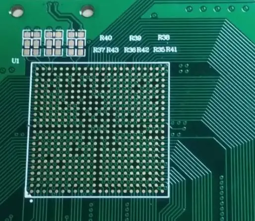
When making PCBs, whether to use double-sided boards or multi-layer boards depends on the maximum operating frequency, the complexity of the circuit system, and the requirements for assembly density. When the clock frequency exceeds 200MHz, it is best to choose multi-layer boards. If the operating frequency exceeds 350MHz, it is best to use printed circuit boards with polytetrafluoroethylene as the dielectric layer, as they have lower high-frequency attenuation, smaller parasitic capacitance, faster transmission speed, and lower power consumption due to larger Z0. The routing of printed circuit boards has the following principles:
(1) All parallel signal lines should be spaced as far apart as possible to reduce crosstalk. If there are two signal lines that are close together, it is best to run a ground line between them for shielding purposes.
(2) When designing signal transmission lines, avoid sharp turns to prevent sudden changes in transmission line characteristic impedance that can cause reflections. Try to design them as uniform arc lines of a certain size.
(3) The width of the printed lines can be calculated based on the above microstrip line and strip line characteristic impedance formulas. The characteristic impedance of microstrip lines on printed circuit boards is generally between 50-120Ω. To achieve a large characteristic impedance, the line width must be very narrow, but very thin lines are also difficult to manufacture.
Considering various factors, a characteristic impedance value of around 68Ω is generally more suitable, as it achieves an optimal balance between delay time and power consumption. A 50Ω transmission line will consume more power; while a larger impedance will reduce power consumption, it will increase transmission delay time.
Negative line capacitance can cause increased transmission delay time and reduced characteristic impedance. However, lines with very low characteristic impedance have a larger intrinsic capacitance per unit length, so their transmission delay time and characteristic impedance are less affected by load capacitance. An important feature of properly terminated transmission lines is that branch short lines should have no effect on line delay time. When Z0 is 50Ω, the length of branch short lines must be limited to within 2.5cm to avoid significant ringing.
(4) For double-sided boards (or four-layer lines in six-layer boards), lines on both sides of the circuit board should be perpendicular to each other to prevent mutual induction from causing crosstalk.
(5) If large current devices such as relays, indicator lights, speakers, etc., are installed on the printed board, their ground lines should be kept separate to reduce noise on the ground line. The ground lines of these large current devices should be connected to an independent ground bus on the plug-in board and backplane, and these independent ground lines should also connect to the system’s ground point.
(6) If the board has small signal amplifiers, the weak signal lines before amplification should be kept away from strong signal lines, and routing should be as short as possible. If possible, ground lines should be used for shielding.
Source: Fanyi PCB
Copyright Statement: This article’s copyright belongs to the original author and does not represent the views of the association. Articles forwarded by the “Jiangxi Province Electronic Circuit Industry Association” are for sharing purposes only and do not represent the position of this account. If there are copyright issues, please contact us for deletion.