PCB Layout is a meticulous task that involves not only regulatory constraints but also numerous details that engineers need to consider. In this article, we have compiled some critical details to pay attention to in layout design. Let’s see if you are aware of them!
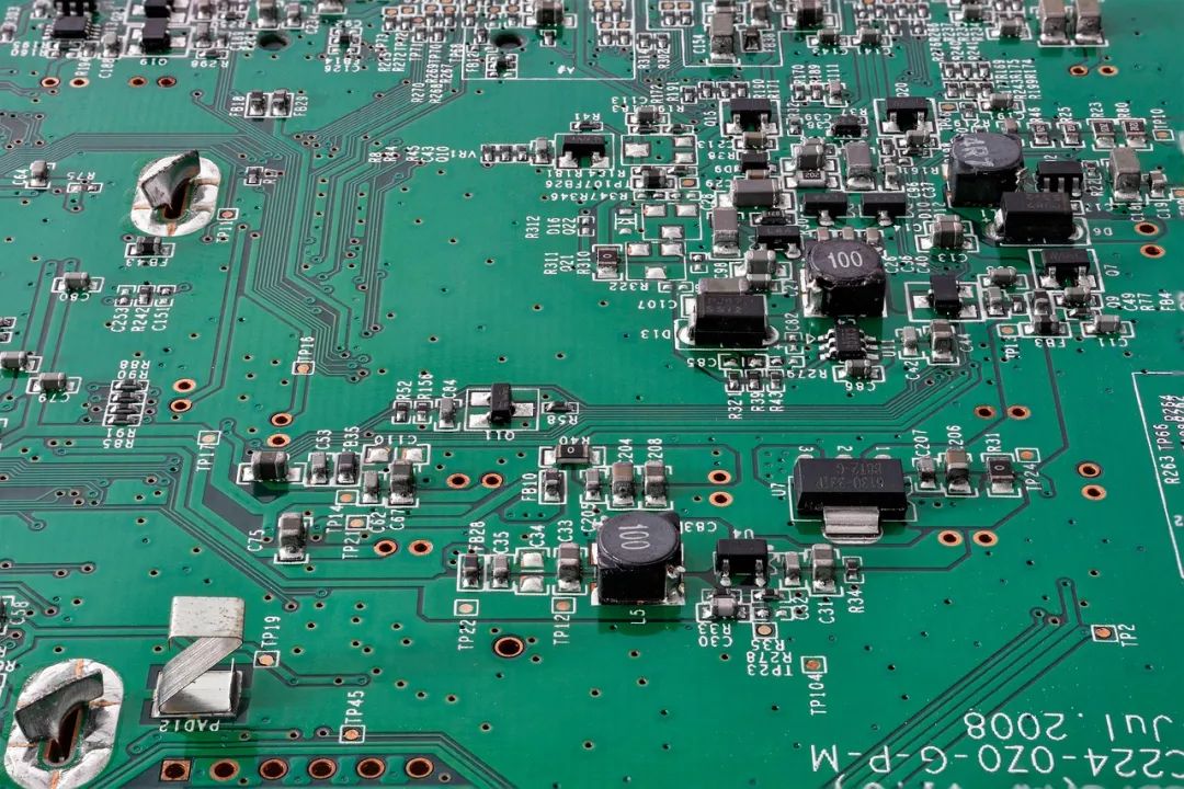
1. Layout of Special Components
√ Heat-generating components should be placed in areas conducive to heat dissipation, such as the edges of the PCB, and away from microprocessor chips; √ Special high-frequency components should be placed close together to shorten their connections; √ Sensitive components should be kept away from noise sources such as clock generators and oscillators; √ The layout of adjustable components like potentiometers, adjustable inductors, variable capacitors, and push-button switches should meet the structural requirements of the entire device for ease of adjustment; √ Heavier components should be secured with brackets; √ EMI filters should be placed close to EMI sources.
2. Placement of Crystals
√ Crystals, made of quartz, are susceptible to external impacts or falls, so they should not be placed at the edges of the PCB; they should be positioned as close to the chip as possible. √ Crystals need to be kept away from heat sources, as high temperatures can also affect their frequency offset.
3. Decoupling Capacitor Rules
It is essential to add necessary decoupling capacitors on the printed circuit board to filter out interference signals from the power supply, ensuring stable power signals. It is recommended that the power supply connects to the power pin after passing through the filter capacitor.
4. Placement of Decoupling Capacitors for ICs
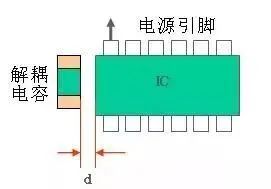
Decoupling capacitors need to be placed near the power ports of each IC, as close to the IC’s power port as possible. When a chip has multiple power ports, decoupling capacitors must be arranged for each port.
5. Keep Electrolytic Capacitors Away from Heat Sources

During design, PCB engineers must first consider whether the environmental temperature for electrolytic capacitors meets requirements, and then ensure that the capacitors are as far away from heat-generating areas as possible to prevent the internal liquid electrolyte from drying out.
6. Spacing Between SMDs
The spacing between surface-mounted components is a critical issue engineers must pay attention to during layout. The spacing should not be too large (which wastes board space) or too small to avoid solder paste printing adhesion and difficulties in soldering repairs.
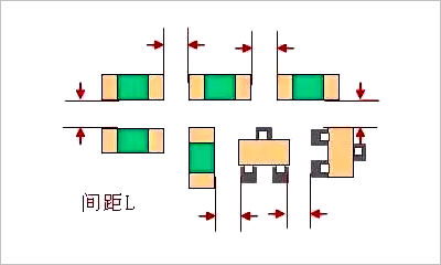 The spacing can refer to the following specifications: √ Same component: ≥ 0.3mm √ Different components: ≥ 0.13×h+0.3mm (h is the maximum height difference between neighboring components) √ For manual soldering and SMD, the distance requirement is: ≥ 1.5mm. (For reference only, it can be designed according to each company’s PCB process specifications.)
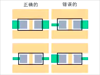
7. Consistent Width of Component Leads
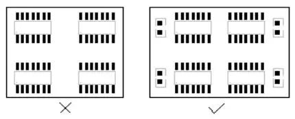
8. Retain Unused Pin Pads
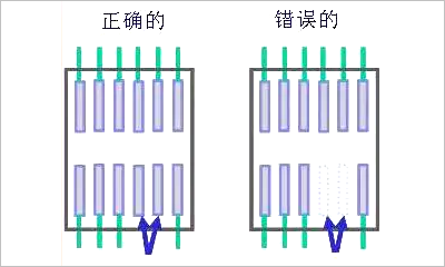 For example, in the case of a chip with two unused pins, the actual chip pins still exist. If the two pins are left floating as shown on the right, it may easily cause interference. If the chip pins are internally unconnected (NC), adding pads and grounding them can help avoid interference.
9. Use of Vias Requires Caution
In almost all PCB layouts, vias must be used to provide electrical connections between different layers. PCB design engineers need to be particularly careful, as vias can introduce inductance and capacitance. In some cases, they can also cause reflections due to changes in characteristic impedance when vias are made in the traces. It is also important to remember that vias increase trace length, requiring matching. For differential pairs, vias should be avoided as much as possible. If unavoidable, vias should be used on both traces to compensate for delays in the signal and return path.
10. Barcode Silk Screen Setup
1) Barcodes should be placed horizontally/vertically. 2) The position of the barcode should not cover pads, test holes, or be obscured by pull tabs, and should facilitate reading of information. 3) At least 5mm from the board edge and 15mm from the pull tab. The preferred placement order is as shown in the figure below: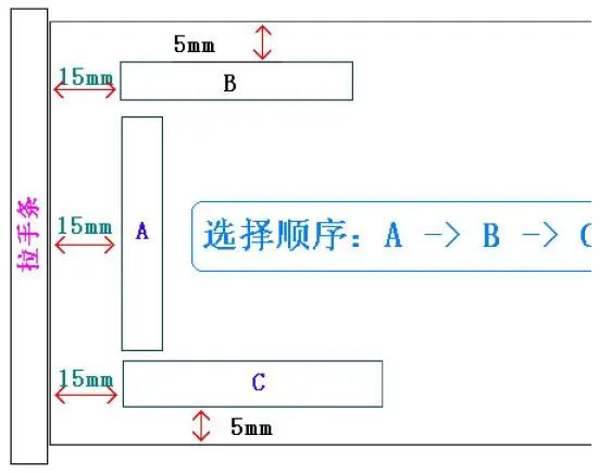 Preferred order for barcode silk screen placement4) For single-sided component boards: solid line frame on the top side → dashed line frame on the top side; for double-sided component boards: both should be solid line frames. 5) Preferred sizes for barcode silk screen frames: 42*8mm → 42*6mm → 7*9mm. 42*8 is suitable for boards passing through automatic lines. (The content is compiled from the internet)