1 Layout Principles
1. Follow the layout principle of “large first, small later; difficult first, easy later,” meaning that important circuit units and core components should be prioritized in layout.
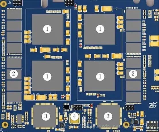
Large first, small later; difficult first, easy later
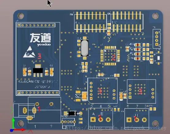
In the above image, 1 is positioned due to mechanical structure determining the power supply and terminal block location.
2. The layout should refer to the schematic diagram, arranging major components based on the main signal flow direction of the board. Layout should aim to meet the following requirements: keep overall wiring as short as possible, with critical signal lines being the shortest; decoupling capacitors should be placed as close as possible to the IC’s power pins, forming the shortest loop with power and ground; reduce unnecessary signal paths to prevent accidents along the way.
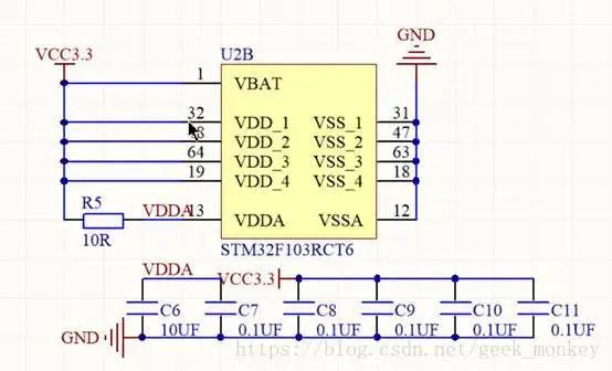
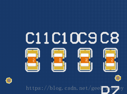
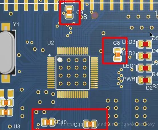
For example, in the image below, C8 to C11 are decoupling capacitors between VCC and GND, and their positional requirements cannot be reflected in the schematic. However, in the PCB, they should be placed near the chip’s power input pins, such as near pins 31 and 32, and also near pins 18 and 19.
Incorrect example, placed side by side
Correct example, close to the chip power input pins
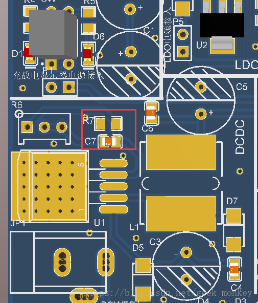
3. The arrangement of components should facilitate debugging and maintenance, meaning that small components should not be placed around large components, and there should be enough space around components that require debugging to avoid a cramped situation, which can be awkward. For example, in the image below, if the surrounding components are soldered first, R7 and C7 will be difficult to solder (this also illustrates the importance of the soldering sequence).
4. For circuit sections with the same structure, a “symmetrical” standard layout should be adopted as much as possible; optimize layout according to uniform distribution, center of gravity balance, and aesthetic appearance.
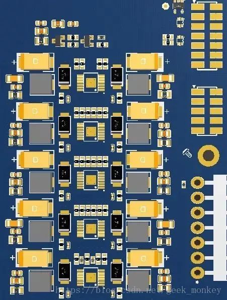
Uniform distribution, center of gravity balance, layout should be neat
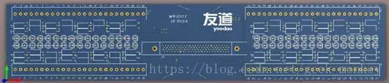
5. Components of the same type should be placed in the same direction along the X or Y axis. Similarly, for polarized discrete components of the same type, strive to maintain consistency in the X or Y direction to facilitate production and inspection (if manual confirmation of component polarity is required, production costs may increase).
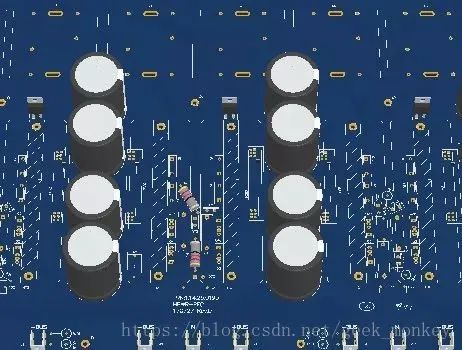
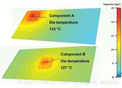
6. Heat-generating components should be evenly distributed to facilitate heat dissipation of the single board and the entire machine; temperature-sensitive components, other than temperature sensing components, should be kept away from high heat-generating components. Besides temperature sensors, transistors are also heat-sensitive components.
7. High voltage, high current signals should be completely separated from low current, low voltage weak signals; analog signals should be separated from digital signals; high frequency signals should be separated from low frequency signals; the spacing between high frequency components should be sufficient. When laying out components, consideration should be given to placing devices that use the same power supply together for future power separation.
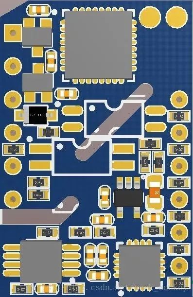
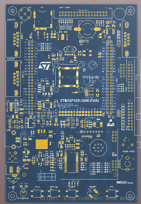
PCB Layout Example
2 Wiring Principles
The above outlines the main considerations for “how to arrange” or layout. Regarding “how to connect,” it is relatively more complex, generally speaking:
-
Priority for key signal lines: prioritize wiring for key signals such as analog small signals, high-speed signals, clock signals, and synchronous signals;
-
Density priority principle: start wiring from the most complexly connected devices on the board. Begin wiring from the area with the densest connections on the board.
The self-service guide for wiring can be summarized as follows:
1. Provide dedicated wiring layers for key signals such as clock signals, high-frequency signals, and sensitive signals, ensuring the smallest loop area possible. If necessary, methods such as manual priority wiring, shielding, and increasing safety spacing should be employed to ensure signal quality.
2. The EMC environment between the power layer and ground layer is poor, so avoid placing interference-sensitive signals.
3. Networks with impedance control requirements should be wired according to line length and width requirements.
3 Example of Layout Based on Schematic
If the layout is inappropriate, using the board may be very inconvenient, and wiring will be difficult.
When laying out, components that complete a certain function should be placed as close as possible to each other, with operational techniques, which will be illustrated with examples next.
First, find the op-amp module components in the schematic and select them while holding down Ctrl.
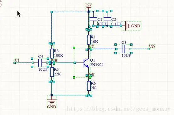
In the PCB, these components have also been selected

Then observe the connection relationships in the schematic, for example, C4 connects to R3, R5, Q1. Find these components in the PCB and place them together.
Observe the pre-wiring situation, knowing that each component has a common network called VB, you can select a pad with the network property of VB while holding down Ctrl, and then VB will be highlighted, for example:
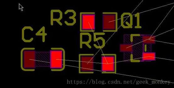
After adjustment, the programming layout is as follows
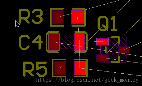
Observe in the schematic, Q1 connects to R6, then drag R6 over as well
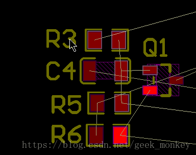
Other components follow this pattern
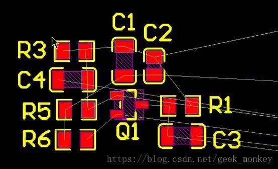
Then wiring can proceed smoothly
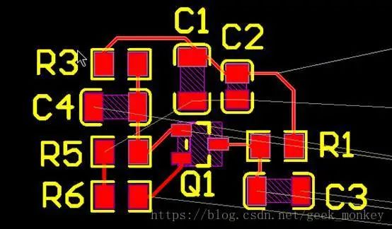
4 Low-Frequency Double-Sided Board Wiring Example
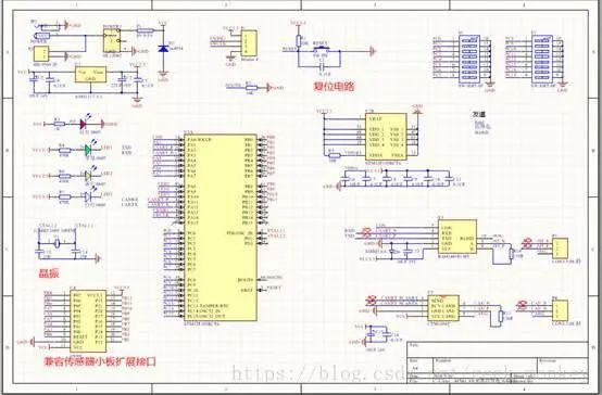
After importing components into the PCB, first complete the layout as required.
Then for signal lines, whether serial, 485, or CAN, the signal lines should be as short as possible, with fewer vias, and sometimes length matching is needed, such as for differential pairs. Additionally, clock lines, such as crystal oscillators, should also be short with fewer vias.
1 First route signal and clock lines.
2 Route power lines, two types of power, VCC and VCC3.3. A specific width rule can be set for power lines. Power lines should also have fewer vias; if necessary, multiple vias can be paralleled.
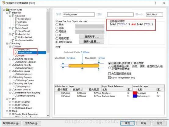
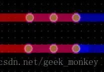
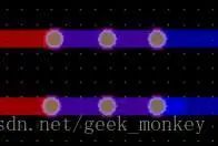
3 Ground lines can be determined based on the situation. For large area copper pours, consider not routing ground lines. If grounding is necessary, the line width should meet the following relationship:
Ground line > Power line > Signal line
4 Other lines should be observed to ensure that horizontal and vertical lines are on different layers as much as possible.
Horizontal lines and vertical lines should be on different layers
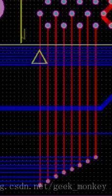
Adjusting the direction of components can facilitate wiring.
Lines that are close to the destination should be neat. An interactive multi-line connection tool can be used.

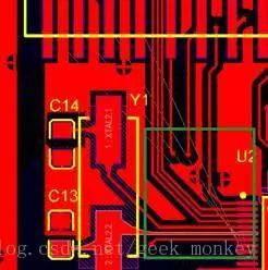
If lines inevitably cross, consider making larger loops (of course, taking the line properties into account).
For example, the flying line has crossed. It can be looped.
Copyright statement: This article is copyrighted by the original author and does not represent the views of the association. Articles pushed by the “Jiangxi Province Electronic Circuit Industry Association” are for sharing purposes only and do not represent the stance of this account. If there are copyright issues, please contact us for deletion.