Detailed Explanation of the Significance of Each Layer in PCB Design
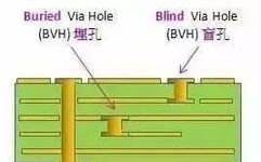
1. Signal Layers Altium Designer can provide up to 32 signal layers, including the Top Layer, Bottom Layer, and Mid-Layers. These layers can be interconnected through vias, blind vias, and buried vias. Figure 1 PCB Holes (1) Top Signal Layer Also known as the component layer, it is mainly used to place components. For double-sided … Read more