1. Signal Layers
Altium Designer can provide up to 32 signal layers, including the Top Layer, Bottom Layer, and Mid-Layers. These layers can be interconnected through vias, blind vias, and buried vias.
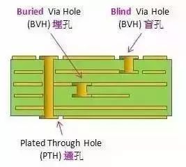
Figure 1 PCB Holes
(1) Top Signal Layer
Also known as the component layer, it is mainly used to place components. For double-sided and multi-layer boards, it can be used to route wires or copper areas.
(2) Bottom Signal Layer
Also known as the solder layer, it is primarily used for wiring and soldering. For double-sided and multi-layer boards, it can be used to place components.
(3) Mid-Layers
Up to 30 layers can exist, used for routing signal lines in multi-layer boards, excluding power and ground lines.
2. Internal Planes
Commonly referred to as internal power layers, they only appear in multi-layer boards. The total number of layers in a PCB typically refers to the sum of signal layers and internal power layers. Similar to signal layers, internal power layers can connect with each other and with signal layers through vias, blind vias, and buried vias.
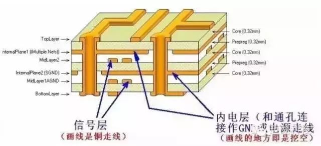
Figure 2 PCB Layer Designations
3. Silkscreen Layers
A PCB can have up to 2 silkscreen layers, namely the Top Overlay and Bottom Overlay, typically in white, used to place printed information such as component outlines and labels, as well as various annotation characters, facilitating component soldering and circuit inspection.
(1) Top Overlay
Used to annotate the projection outlines of components, component designations, nominal values or models, and various annotation characters.
(2) Bottom Overlay
Similar to the Top Overlay; if all annotations in the Top Overlay are included, the Bottom Overlay can be disabled.
4. Mechanical Layers
Mechanical layers are generally used to place indicative information regarding board fabrication and assembly methods, such as PCB dimensions, dimension markings, data materials, via information, assembly instructions, etc. This information varies according to the requirements of design companies or PCB manufacturers. Below are examples of our common methods.
Mechanical 1: Generally used to draw the PCB’s border, serving as its mechanical outline, thus also referred to as the outline layer;
Mechanical 2: Used to place the PCB processing requirements table, including dimensions, materials, layers, etc.;
Mechanical 13 & Mechanical 15: Contains the physical dimensions of most components in the ETM library, including the 3D models of components; this layer is by default not displayed for page simplicity;
Mechanical 16: Contains the footprint area information of most components in the ETM library, useful for estimating PCB dimensions in the early stages of a project; this layer is also by default not displayed and is colored black.
5. Mask Layers
Altium Designer provides two types of mask layers: solder mask and paste mask, each with top and bottom layers, which will not be elaborated here.