With the rapid development of the PCB industry, PCBs are gradually moving towards high-precision fine lines, small apertures, and high aspect ratios (6:1-10:1). The copper requirement for holes is 20-25μm, and for boards with DF line spacing ≤4 mil, most PCB manufacturers face plating film issues. Film entrapment can cause direct short circuits, affecting the first-pass yield of PCBs during AOI inspection, and severe film entrapment or excessive spots that cannot be repaired directly lead to scrapping.
Diagram Illustrating Plating Film Issues: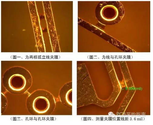 Analysis of PCB Film Entrapment Principles① If the thickness of the patterned electroplated copper is greater than the dry film thickness, it will cause film entrapment. (Generally, the dry film thickness used by PCB manufacturers is 1.4 mil)② If the thickness of the patterned electroplated copper plus the thickness of tin exceeds the dry film thickness, it may cause film entrapment.Analysis of PCB Film Entrapment Causes
1. Images and Photos of Boards Prone to Film Entrapment
 From images three and four, it can be seen that the lines are densely packed, and the aspect ratio of the engineering design layout differs significantly, which is detrimental to current distribution. The minimum line gap for D/F is 2.8 mil (0.070mm), the minimum hole is 0.25mm, and the board thickness is 2.0mm, with an aspect ratio of 8:1. The copper requirement for holes is >20μm. This belongs to a high-difficulty board process. 2. Analysis of Film Entrapment Causes① High current density in patterned electroplating, resulting in excessive copper deposition.② No edge strips at both ends of the flying bar, leading to thick deposition in high current areas causing film entrapment.③ The transformer setting current is larger than the actual production board.④ The C/S and S/S sides are reversed.⑤ Gap too small, boards with spacing of 2.5-3.5 mil prone to film entrapment.⑥ Uneven current distribution, copper plating tanks not cleaned for long periods.⑦ Incorrect current settings (wrong model or incorrect board area input).⑧ Equipment failure, PCB boards in copper tanks protected for too long.⑨ Unreasonable engineering layout design, incorrect effective electroplating area provided by engineering, etc.⑩ PCB board line gaps are too small; high-difficulty board line patterns are particularly prone to film entrapment.
Effective Improvement Measures for Film Entrapment
1. Reduce the current density for patterned electroplating and appropriately extend the copper plating time.
2. Increase the thickness of the copper plating on the board appropriately, while reducing the current density of the patterned electroplating to relatively decrease the thickness of the patterned electroplated copper.
3. Change the base copper thickness from 0.5 OZ to 1/3 OZ for the base copper pressing plate. Increase the thickness of the copper plating on the board by about 10μm, reduce the current density for patterned electroplating, and decrease the thickness of the patterned electroplated copper.
4. For boards with spacing <4 mil, purchase 1.8-2.0 mil dry film for trial production.
5. Other solutions such as redesigning layout, modifying compensation, moving line gaps, and adjusting hole rings and pads can also relatively reduce the occurrence of film entrapment.
Control Methods for Electroplating Production of Boards with Small Line Gaps
1. FA: First, test a flying bar board with edge strips at both ends. After ensuring copper thickness, line width/spacing, and impedance are qualified, etch the flying bar board and pass AOI inspection. If film entrapment is found, immediately adjust the current and retest FA.
2. Stripping: For D/F line gaps <4 mil, slow down the etching and stripping speed appropriately.
3. Skills of FA personnel: When producing boards prone to film entrapment, pay attention to current density evaluation when current indicators are displayed. Generally, for boards with minimum line gaps <3.5 mil (0.088mm), control the current density for patterned electroplated copper at ≦12 ASF to avoid film entrapment. Except for especially high-difficulty board line patterns as shown below:
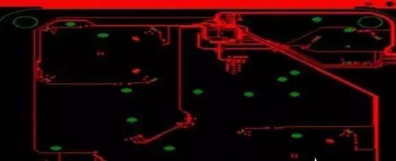
This patterned board has a minimum D/F line gap of 2.5 mil (0.063mm). Even under good uniformity conditions of the manufacturer’s electroplating line, it is difficult to escape the fate of film entrapment. It is recommended to use ≦10 ASF current density for patterned electroplating during FA.
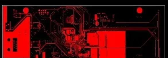
This patterned board has a minimum D/F line gap of 2.5 mil (0.063mm), with many independent lines and uneven distribution. Even under good uniformity conditions of the manufacturer’s electroplating line, it is difficult to escape the fate of film entrapment. The current density for copper plating in patterned electroplating was 14.5 ASF for 65 minutes with film entrapment; it is recommended to use ≦11 ASF current density for patterned electroplating during FA.Personal Insights and SummaryBased on my years of experience in PCB processes, almost every PCB factory faces some degree of film entrapment issues when producing boards with small line widths and gaps. The difference lies in the varying proportions of film entrapment defects in each factory; some companies have very few issues, while others have more. The following factors are analyzed: 1. Each company’s PCB board structure types differ, leading to different manufacturing process difficulties. 2. Each company’s management models and operational methods differ. 3. From my years of accumulated experience and research, for boards with small gaps, it is crucial to use only low current densities and appropriately extend copper plating time. Evaluate the current indicators based on experience to determine the appropriate current density and copper plating time, paying attention to the clamping method and operation methods. For boards with minimum line spacing ≤4 mil, the flying bar board must pass AOI inspection for any film entrapment issues, which also serves quality control and preventive purposes. This way, the likelihood of film entrapment during mass production will be minimized. I believe that ensuring PCB quality requires not only experience and skills but also good methods. Additionally, the execution strength of production personnel plays a significant role. Patterned electroplating differs from whole board electroplating, mainly in that various model boards’ line patterns need to be plated. Some boards have uneven line distributions, in addition to fine line widths and gaps, there are sparse lines, isolated lines, and various special line patterns. Therefore, I prefer to use FA (current indication) skills to solve or prevent the issue of excessive film entrapment. Small adjustment actions yield quick results, and the preventive effect is significant.
Source: Internet