1. Common Shortcuts in PCB
R+L outputs the wiring length of all networks in the PCB.
Ctrl + Left Click completes the auto-routing connection for the line being routed.
M + G can change the shape of copper.
Press P + T while routing, then Shift + A for direct serpentine routing.
T + R performs serpentine routing on already routed lines.
E + M + C quickly finds the desired component on the PCB by clicking on a blank space.
Backspace undoes the last operation while routing.
* Switch routing layers, allowing via placement during routing.
Ctrl + Shift switches layers and places vias.
F8 / E + O + S sets the center point.
M + I flips the selected component.
P + T for routing.
T + E for adding teardrops.
P + G for copper pouring.
S + Y for single-layer line selection.
E + B for selecting to copy.
2. Summary:
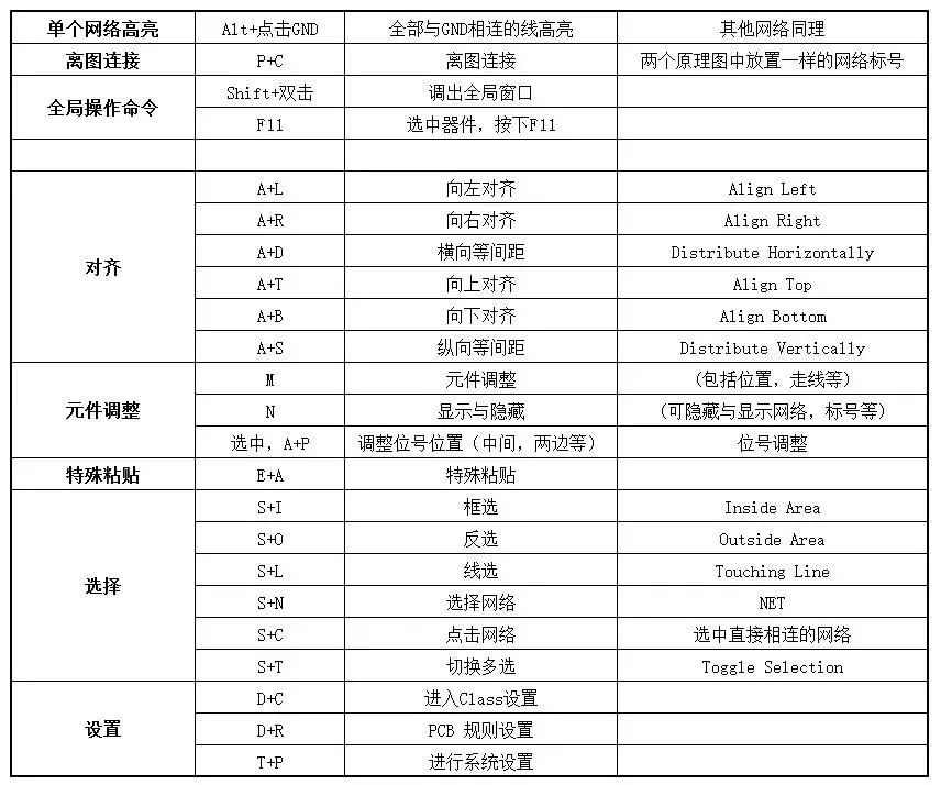
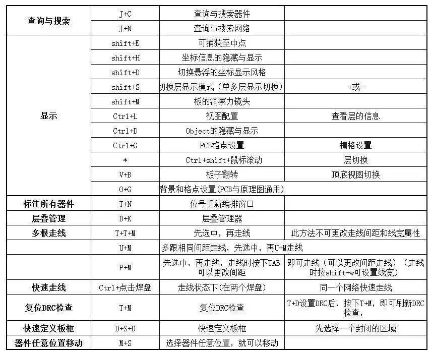
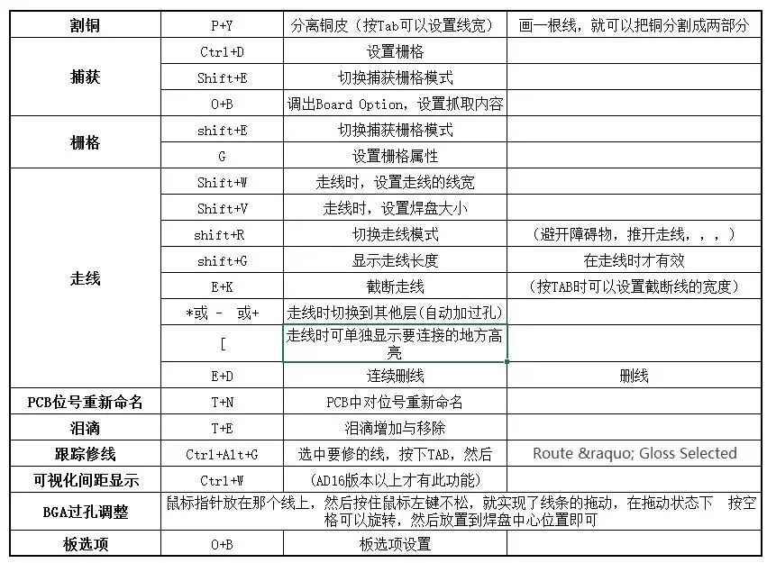
3. Considerations for BGA Fan-Out

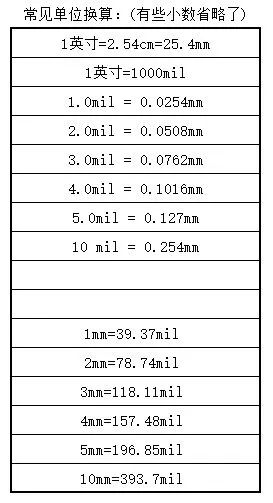
4. Common Unit Conversions


To facilitate better learning for everyone, Changxue Electronics Network has specially added a public account focused on microcontrollers and EDA, pushing relevant knowledge daily, hoping to assist your learning!