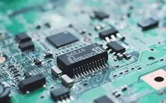
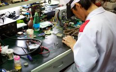
How Engineers Can Effectively Debug PCB Circuit Boards
In the field of electronic engineering, debugging (Debug) circuit boards is an indispensable part of the product development process, directly related to whether the product’s functions and performance meet the standards. In the face of complex digital circuit systems, an efficient and organized Debug process is particularly important. So how can we effectively perform its … Read more