1
Bridge Connection
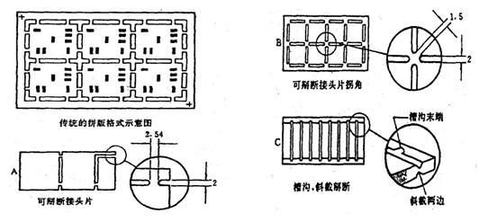
The bridge connection point is a high-stress area on the PCB, which can easily cause cracking or fractures in surrounding solder joints and components.The length of the bridge connection point should be <2.54mm and the width <2mm.As shown in the figure below.
2
V-Groove
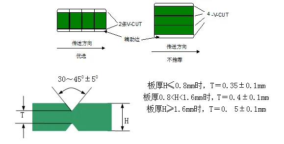
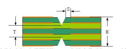
① The thickness of the PCB for stacking should be ≤3.5mm.The number of V-groove lines in the parallel transport direction should be ≤3 (exceptions can be made for elongated boards). For irregular stacking, when using the milling groove plus V-CUT method, the milling groove spacing should be ≥2.0mm. The thickness for double-sided V-groove milling—slotting or connecting should be 1/3 of the board thickness, with an error of ±0.15mm; the angle should be 30°/45°±5°. The positioning accuracy deviation of the upper and lower cutters should be ±0.076mm. As shown in the figure below.
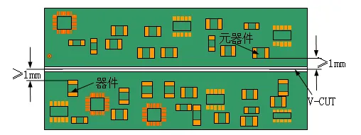
② For PCBs that require automatic board separation, the V-CUT lines on both sides (TOP and BOTTOM) must each reserve a component prohibition area of no less than 1mm to avoid damaging components during automatic board separation. As shown in the figure below. (The components conflict with V-CUT and 5.3.7)
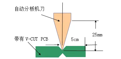
③ It is also necessary to consider the structure of the blade of the automatic board separation machine, as shown in the figure below. Within a range of 5mm from the component prohibition area at the edge of the board, components with a height exceeding 25mm are not allowed to be placed.
④ The safe distance “S” from the edge of the V-CUT to the edge of the circuit (or PAD) must be considered, to prevent damage to the circuit or exposed copper. Generally, it is required that S≥0.3mm. As shown in the figure below.
3
Stamp Hole
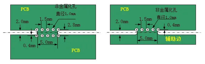
Note that the edge connections should be evenly distributed around each stacked board to avoid deformation during soldering due to uneven stress on the PCB. The stamp holes should all be non-metalized holes, with a hole diameter of 1mm, and the center distance between holes should be 1.6 to 2mm. It is recommended that the distance between two sets of stamp holes be 50mm. The stamp holes should be placed at the edge of the main board, with the hole center located at the edge of the main board, and should not be placed at the corners. As shown in the figure below.
 Source: Electronic Engineering Magazine
Disclaimer: The copyright of this article belongs to the original author and does not represent the views of the association. The articles forwarded by the “Jiangxi Province Electronic Circuit Industry Association” are for sharing purposes only and do not represent the position of this account. If there are any copyright issues, please contact us for deletion.