Analysis and Optimization of Copper Plating Voids in Small Diameter PCB Through-Holes

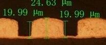
In PCB manufacturing, the occurrence of voids in small diameter through-hole copper plating is indeed a troublesome issue, as it directly affects the reliability of the circuit and the yield of the product. This is often the result of multiple factors working together. The table below summarizes the common causes of copper plating voids and … Read more