Welcome FPGA engineers to join the official WeChat technical group.
This article mainly introduces the configuration modes of Xilinx FPGAs, including Master/Slave mode, Serial/SelectMAP mode, JTAG mode, etc. Among them, the 7 series only has the Logic part, and all configuration-related function pins are connected to specific banks on the FPGA side; the Zynq 7000 series has both PL and PS parts, with JTAG drawn from the PL side, and the remaining configuration-related pins drawn from the PS side; the Zynq UltraScale+ series also has PL and PS parts, but all configuration-related function pins are drawn from the PS side.
1. 7 Series Configuration
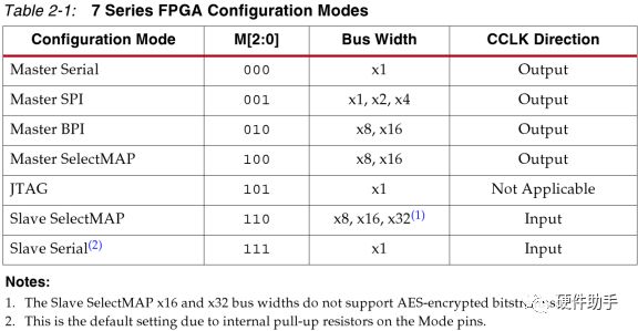
The configuration modes supported by the 7 series FPGA are shown in the table below, so the bank locations for each series are different, and the interface voltages are also different.
The pin definitions corresponding to each mode are shown in the table below:
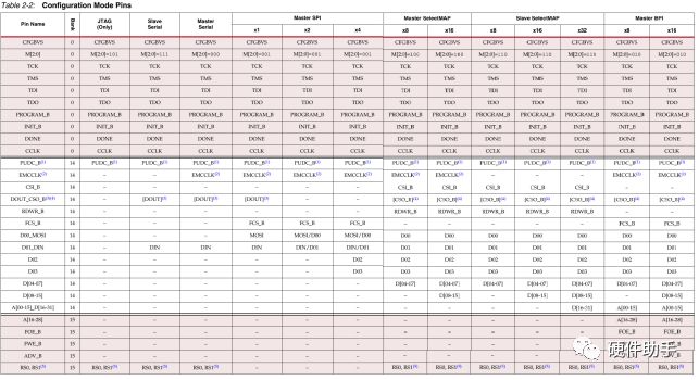
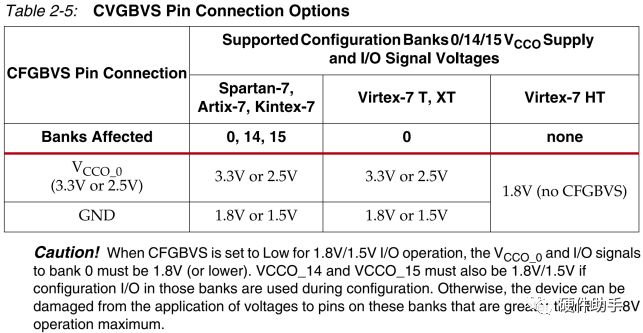
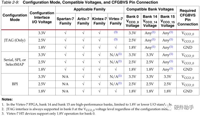
The definitions for each configuration pin are not listed one by one in this article; please refer to Table 2-4 in UG470 for details. The voltage selection pins for the configuration banks are detailed below:
There are many specific configuration modes, each with a connection diagram; please refer to the figures in UG470, such as Figure 2-2 (Slave Serial Mode), Figure 2-5 (Single Slave Device SelectMAP Mode), Figure 2-12 (Master SPI x1/x2 Mode), Figure 2-14 (Master SPI x4 Mode), Figure 2-17 (Master BPI Mode-Asynchronous), and Figure 2-20 (Master BPI Mode-Synchronous). Additionally, Master Serial Mode is similar to Slave Serial Mode, except that CCLK is generated by the FPGA.
2. UltraScale Series Configuration
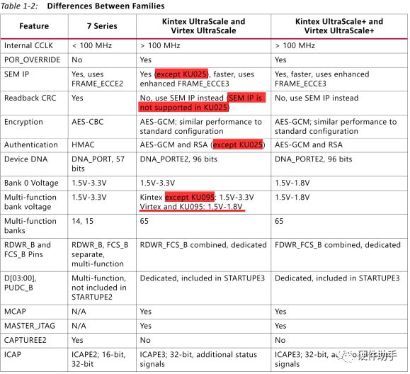
The configuration of UltraScale series FPGAs is similar to that of the 7 series, with the main differences shown in the table below:
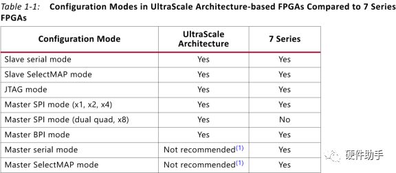
The supported configuration modes are shown in the table below:
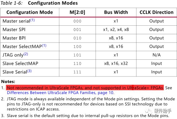
The pin definitions corresponding to each mode are shown in the table below:
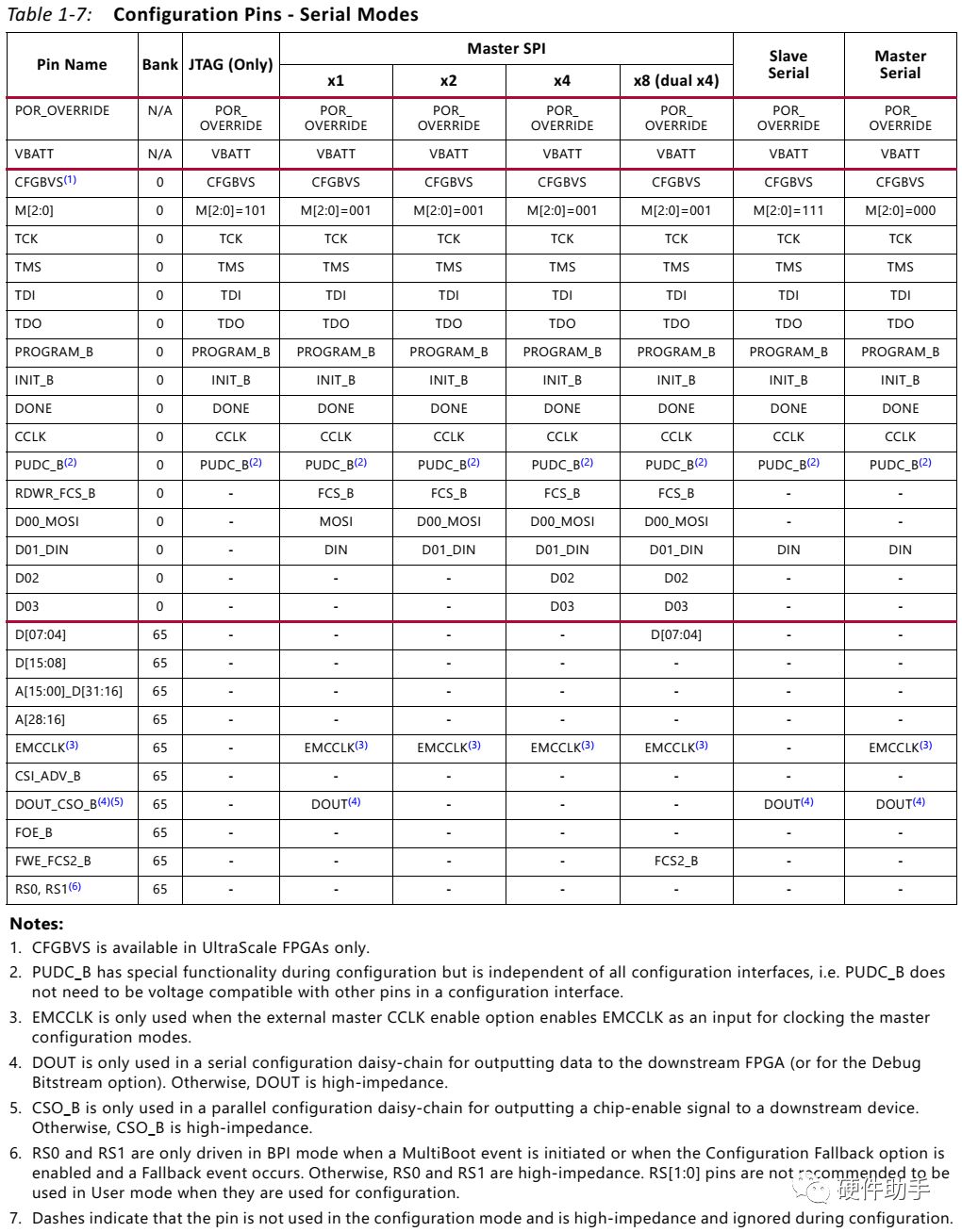
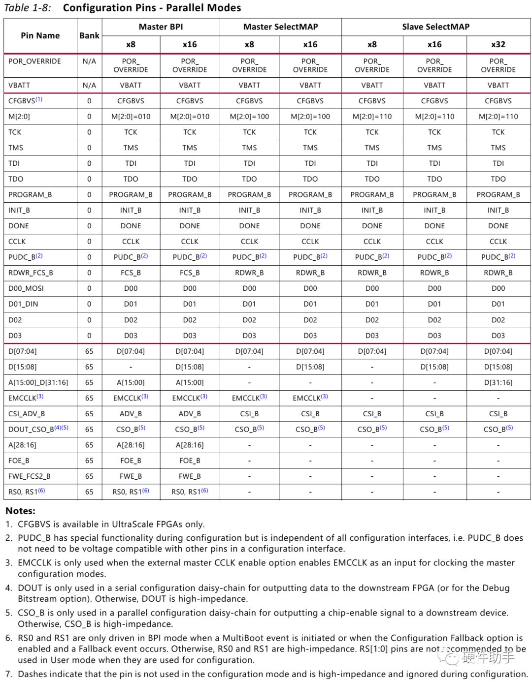
The definitions for each configuration pin are not listed one by one in this article; please refer to Table 1-9 in UG570 for details. The voltage selection pins for the configuration banks are detailed below:
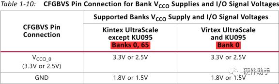
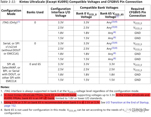
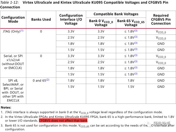
There are many specific configuration modes, each with a connection diagram; please refer to the figures in UG570, such as Figure 2-2 (Master SPI x1/x2 Mode), Figure 2-4 (Master SPI x4 Mode), Figure 2-5 (Master SPI x8 Mode), Figure 3-2 (Slave Serial Mode), Figure 4-2 (Master BPI Mode-x16 Synchronous), Figure 4-4 (Master BPI Mode-x16 Synchronous), and Figure 5-2 (Slave SelectMAP Mode).
3. UltraScale+ Series Configuration
The basic configuration of UltraScale+ series is similar to that of UltraScale series, with the following main differences:
-
Master serial and master SelectMAP configuration modes are not supported in the UltraScale+ FPGAs. These modes are not recommended in the other UltraScale families. (US+ does not support Master Serial and Master SelectMAP modes.)
-
The configuration interface can operate only at 1.8V or 1.5V in the UltraScale+ FPGAs. There is no CFGBVS pin in UltraScale+ devices. When migrating from an UltraScale FPGA to an UltraScale+ FPGA, the CFGBVS pin location becomes RSVDGND and must be connected to GND. (US+ configuration interface only supports 1.8V and 1.5V, there is no CFGBVS pin, but a reserved RSVDGND pin, which must be grounded to ensure compatibility with previous US series.)
-
There is no CFGBVS pin in the Kintex UltraScale+ and Virtex UltraScale+ FPGAs because their configuration I/O only support operation at 1.8V or 1.5V. The pin location is labeled RSVDGND and it must be connected to GND.
-
The configuration timing and configuration rate options are different between UltraScale FPGAs and UltraScale+ FPGAs. The configuration frame size is 93 32-bit words in the UltraScale+ FPGAs and 123 32-bit words in the UltraScale FPGAs. (The configuration bitstream size is different.)
-
Bank 65 is an HR bank in most Kintex UltraScale FPGAs (except KU095), an HP bank in the KU095 and Virtex UltraScale FPGAs, and an HP bank in all Kintex UltraScale+ and Virtex UltraScale+ FPGAs.
4. Z7 Series Configuration
The configuration part of the Zynq 7000 series SoC is entirely on the ARM side. In addition to JTAG drawn from the FPGA side (although JTAG is drawn from the FPGA side, the PS part can be configured in Cascade mode, forming a JTAG chain between the PL side and the PS side), its configuration follows the ARM processor’s configuration. The supported modes are shown in the table below:
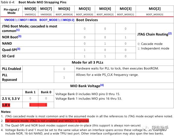
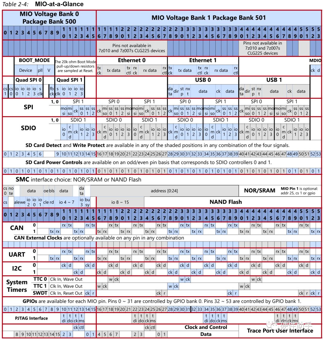
The pin definitions corresponding to each peripheral interface are shown in the table below:
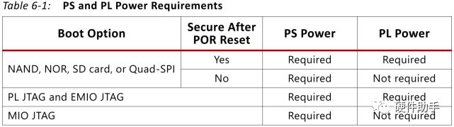
The power requirements vary under different modes,
The handling of configuration-related pins is as follows:
-
MIO[8:2] is used to configure the boot mode, PLL bypass, and MIO voltage. All designs must include a 20 KΩ pull-up or pull-down resistor on these pins to set the required setting. (The external configuration pins use a 20K resistor for pull-up or pull-down processing.)
-
MIO[8] is a dual-use pin that is shared with the high-speed QSPI/NAND/SRAM interface signals. Special care needs to be taken to avoid signal integrity issues. To avoid signal integrity issues, limit the stub length to the pull-up or pull-down resistor to < 10 mm, at the same time, 20.5K resistors must be placed near the middle of QSPI traces. (MIO[8] is a multifunction pin; special attention is needed to ensure signal integrity.)
-
When system design requires the modes to be changeable, it is recommended to not use a resistor tree to set the mode but instead connect one pull-up/down resistor to the mode pin and place a jumper on the other side of the resistor to select between pull-up or pull-down. (To facilitate switching boot modes, a pull-up/down approach can be reserved; a switch can also be used.)
-
The PL system JTAG interface, PL_JTAG, should have its signals TDI, TMS, and TCK pulled-up. (The actual chip has pull-ups inside.)
Below is a detailed introduction to SPI, NAND, NOR, SD Card, and JTAG methods:
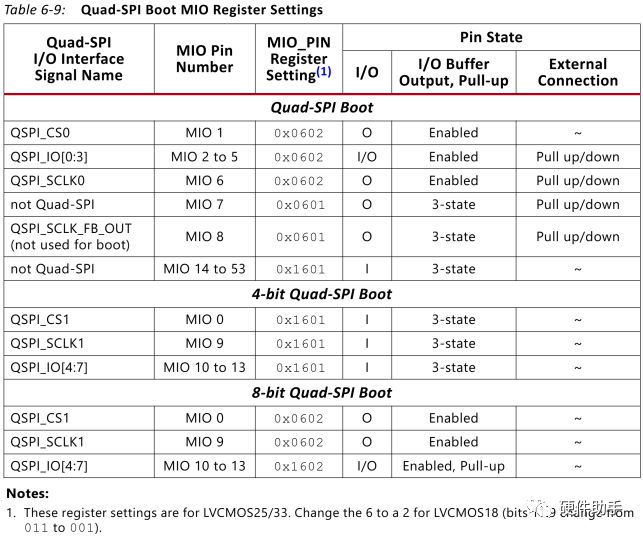
4.1 Quad-SPI Boot
Quad-SPI boot has these features:
-
x1, x2, and x4 single device configuration.
-
Dual SS, 8-bit parallel I/O device configuration.
-
Dual SS, 4-bit stacked I/O configuration.
-
Execute-in-place option.
When using Quad-SPI mode for configuration, if the SPI Flash device uses 24-bit addressing, it can only recognize a maximum of 16MB of SPI Flash. If you want to use SPI Flash larger than 16MB, it must support 32-bit addressing!!!
Specific precautions for SPI boot are as follows:
-
The dual SS, 4-bit stacked I/O device configuration is supported, but the BootROM only searches within the first 16 MB address range. The BootROM accesses the device connected to the QSPI0_SS_B slave select signal.
-
In cases of Quad-SPI boot, if the image is authenticated, then the boot image should be placed at a 32K offset other than 0x0 (the image should not be placed starting at 0x0 offset in Quad-SPI).
-
There are special reset requirements when using more than 16 MBs of Flash memory. For hardware, refer to AR# 57744 for information. For software considerations, refer to UG821, Zynq-7000 All Programmable SoC Software Developers Guide.
-
Boot Image requirements when using larger than 16MB QSPI and RSA Authentication (refer AR# 57900).
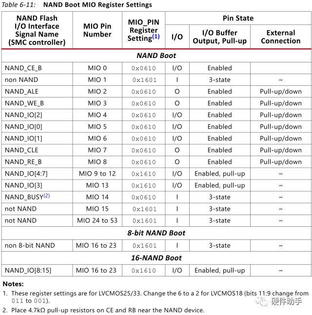
4.2 NAND Boot
NAND boot has these features:
-
8-bit or 16-bit NAND flash devices
-
Supports ONFI 1.0 device protocol
-
Bad block support
-
1-bit hardware ECC support
Precautions during use are as follows:
-
The boot image must be located within the first 128 MB address space of the NAND flash device for the BootROM Header search function.
-
The BootROM reads the ONFI compliant parameter information in 8-bit mode to determine the device width. If the device is 16 bits wide, then the BootROM enables the upper eight I/O signals for a 16-bit data bus. The 16-bit NAND interface is not available in 7z010 dual core and 7z007s single core CLG225 devices.
4.3 NOR Boot
NOR boot has these features:
-
x8 asynchronous flash devices
-
Densities up to 256 Mb
-
Execute-in-place option
Precautions during use are as follows:
-
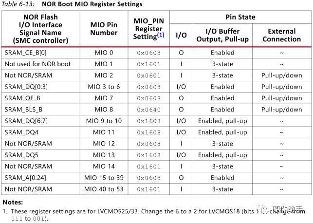
The BootROM does not try to perform any configuration detection of NOR flash devices. When NOR is the selected boot device, the BootROM programs the MIO pins as shown in Table 6-13.
-
The NOR interface is not available in 7z010 dual core and 7z007s single core CLG225 devices.
4.4 SD Card Boot
SD card boot supports these features:
-
Boot from standard SD or SDHC cards
-
FAT 16/32 file system
-
Up to 32 GB card densities
Precautions during use are as follows:
-
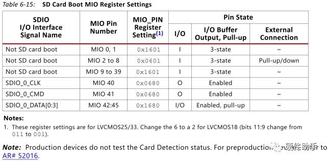
The SD card boot mode is not supported in 7z010 dual core and 7z007s single core CLG225 devices.
-
The SD card boot mode does not support header search or multiboot.
4.5 JTAG
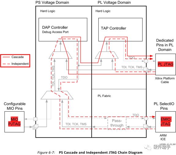
The JTAG part is drawn from the PL side, but the JTAG on the PS side can be drawn from the PL side in Cascade mode, or from MIO/EMIO in Independent mode.
5. ZU+ Series Configuration
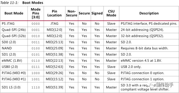
The configuration part of the Zynq UltraScale+ series MPSoC/RFSoC is entirely on the ARM side, so its configuration follows the ARM processor’s configuration. The supported modes are shown in the table below:
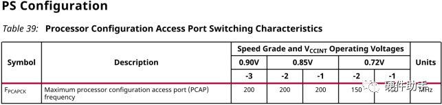
The frequency of the configuration clock has requirements, and the upper limit of the configuration clock frequency varies with different voltage levels.
The handling of Boot Mode pins is as follows:
-
Connect the boot mode pins to a 4.7 kΩ or lower pull-up resistor to VCCO_PSIO[3] or pull-down to ground depending on the desired setting.
-
If multiple switchable boot modes are desired, connect one pull-up/down resistor to the mode pin and place a jumper on the other side of the resistor to select between pull-up or pull-down.
-
An easily switchable boot mode configuration is recommended for debug ease-of-use.
The handling of PS_INIT_B, PS_PROG_B, and PS_DONE pins is as follows:
-
Connect PS_INIT_B to a 4.7 kΩ pull-up resistor to VCCO_PSIO[3]. PS_INIT_B is open drain and should not be driven during logic built-in self test (LBIST).
-
Connect PS_PROG_B to a 4.7 kΩ pull-up resistor to VCCO_PSIO[3]. PS_PROG_B is open drain and should not be driven during LBIST.
-
Connect PS_DONE to a 4.7 kΩ pull-up resistor to VCCO_PSIO[3].
External configuration supports booting via SPI, NAND, SD, eMMC, USB, JTAG, etc., as follows:
-
Quad-SPI (24b/32b): The BootROM code can boot Quad-SPI using 24- or 32-bit addressing.
Image search for multi-boot is supported in this boot mode. The QSPI boot mode also supports x1, x2, and x4 read modes for a single Quad-SPI memory and x8 for a dual QSPI. This is the only boot mode that supports execute-in-place (XIP).
-
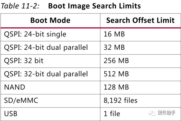
NAND: The NAND boot mode only supports 8-bit widths for reading the boot images. Image search for multi-boot is supported. Boot mode image search limits are 128MB.
-
SD0/SD1: These boot modes support FAT 16/32 file systems for reading the boot images. Image search for multi-boot is supported. The maximum number of files that can be searched as part of an image search for multi-boot is 8,192. The SD supported version is 2.0. It only supports 3.3V for the I/Os and up to 4 bits of data interface.
-
SD1(LS): The SD1-LS boot mode is the same as SD0/SD1 with additional support for the SD 3.0 (with an SD 3.0 compliant voltage level shifter).
-
eMMC(18): This boot mode is the same as the SD boot mode except it only supports 1.8V for the I/Os and up to 8 bits of data interface.
For SD and eMMC boot modes, the boot image file should be at the root of the first partition of the SD card (not inside any directory).
-
USB0: The USB boot mode configures USB controller 0 into device mode and uses the DFU protocol to communicate with an attached host.
The USB host contains the FSBL boot image (e.g., boot.bin) that is loaded into OCM memory for the CSU BootROM code and an all-encompassing boot image file (e.g., boota53_all.bin) that is loaded into DDR memory.
The size of these files is limited by the size of the OCM and DDR memories. The USB boot mode does not support multi-boot, image fallback, or XIP.
The Boot image search limits for each boot mode are shown in the table below:
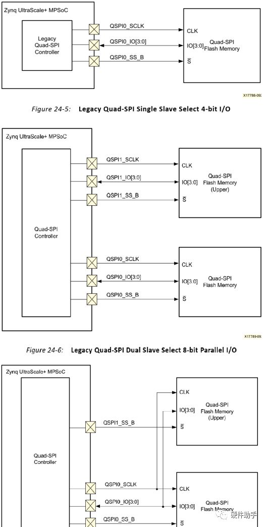
For SPI configuration, when using Quad-SPI mode for configuration, if the SPI Flash device uses 24-bit addressing, it can recognize a maximum of 16MB of SPI Flash. If you want to use SPI Flash larger than 16MB, it must use 32-bit addressing. If you want to use 32-bit addressing, the reset of the SPI Flash must be connected to the reset of the FPGA to ensure that the SPI Flash can be reconfigured when the FPGA is reconfigured.
When using SPI Flash for configuration, since different SPI Flash chips support different maximum configuration clock frequencies, both ZU+ and SPI Flash clock limits must be satisfied.
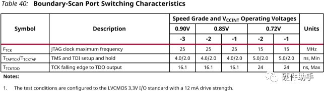
The above is an introduction to the configuration of the 7 Series, UltraScale, UltraScale+, Zynq 7000, and Zynq UltraScale+ series. For more details, please refer to the configuration sections in documents such as UG470, UG570, UG585, and UG1085.

Welcome communication engineers and FPGA engineers to follow our official account.

FPGA WeChat technical group
Welcome everyone to join the national FPGA WeChat technical group, where there is a group of engineers who love technology, and you can discuss technology together!

Press and hold with your finger to join the national FPGA technical group.
FPGA technical group platform is self-operated: Xilinx Altera Micron, Samsung, Hynix, ADI TI ST NXP and other brand advantage distributors. If you have any needs, please send us your model list at any time, and we will provide you with the most competitive quotes as soon as possible! Prices are more than 5% lower than your original suppliers! Welcome to inquire – WeChat: 1051197468 or send your requirements directly to the group owner.
Official thanks to brands: Xilinx, intel (Altera), microsemi (Actel), Lattice, Vantis, Quicklogic, Lucent, etc.