Welcome FPGA engineers to join the official WeChat technical group
ClickBlue TextFollow us at FPGA Home – the best and largest pure engineer community in China for FPGA

This article mainly introduces the power design for Xilinx FPGA, covering types of power supply, voltage requirements, power consumption needs, power-up and power-down timing requirements, and common power implementation solutions.
1. Types of Voltage and Requirements
With the development of FPGA, the types of voltages have become increasingly diverse, mainly including the following types:
-
Processor System voltage, primarily powering the ARM in the Zynq series SoCs, including VCC_PSINTFP, VCC_PSINTLP, VCC_PSAUX, VCC_PSINTFP_DDR, VCC_PSADC, VCC_PSPLL, VPS_MGTRAVCC, VPS_MGTRAVTT, VCCO_PSDDR, VCC_PSDDR_PLL, VCCO_PSIO, VCC_PSBATT, etc.;
-
FPGA Logic voltage, mainly powering the FPGA logic part, including VCCINT, VCCINT_IO, VCCBRAM, VCCAUX, VCCO, VCCAUX_IO, VBATT, etc.;
-
GTx Transceiver voltage, primarily powering the GTx high-speed transceiver of the FPGA part, including VCCINT_GT, VMGTAVCC, VMGTAVTT, VMGTVCCAUX, VMGTAVTTRCAL;
-
System Monitor voltage, primarily powering the ADC of the FPGA part, including VCCADC, VREFP;
-
High Bandwidth Memory voltage, including VCC_HBM, VCC_IO_HBM, VCCAUX_HBM;
-
VCU voltage, available only in devices of the Zynq UltraScale+ MPSoC series with image processing cores, including VCCINT_VCU;
-
RF voltage, available only in the Zynq UltraScale+ RFSoC series, including VADC_AVCC, VADC_AVCCAUX, VDAC_AVCC, VDAC_AVCCAUX, VDAC_AVTT, VCCINT_AMS, VCCSDFEC;
Each of these voltage supplies has different targets and varying precision requirements. For different architectures of FPGA, the precision requirements for voltage also differ, with ripple ranges from 2% to 5%, but overall the requirements are quite high, while the current requirements are increasing, for instance, VCCINT can reach several tens of amps. Moreover, various voltage values differ, some can be combined while others cannot, and timing control is also required.
For Zynq UltraScale+ MPSoC (ZU+ MPSoC), Zynq UltraScale+ RFSoC (ZU+ RFSoC), Zynq 7000 (Z7), UltraScale+ (US+ including VU+ and KU+), UltraScale (US including VU and KU), 7 series, etc., the voltage types and their required values and precision are listed in the following table:
|
Voltage Type |
ZU+ MPSoC |
ZU+ RFSoC |
Z7 |
US+ |
US |
7 Series |
|
|
Logic |
VCCINT |
0.85(3%) 0.72(3%) 0.9(3%) |
0.85(3%) 0.72(3%) |
1.0(3%) 0.95(3%) |
0.85(3%) 0.72(3%) 0.9(3%) |
0.95(3%) 0.9(2.2%)KU 1.0(3%) |
1.0(3%) 0.9(3%) 0.95(2%) AKVThree series differ |
|
VCCINT_IO |
0.85(3%) 0.9(3%) |
0.85(3%) |
× |
0.85(3%) 0.9(3%) |
0.95(3%) 0.9(2.2%)KU 1.0(3%) |
× |
|
|
VCCBRAM |
0.85(3%) 0.9(3%) |
0.85(3%) |
1.0(3%) 0.95(3%) |
0.85(3%) 0.9(3%) |
0.95(3%) 1.0(3%) |
1.0(3%) 0.9(3%) 0.95(3%) AKVThree series differ |
|
|
VCCAUX |
1.8(3%) |
1.8(3%) |
1.8(5%) |
1.8(3%) |
1.8(5%) |
||
|
VCCO |
√ |
√ |
√ |
√ |
√ |
||
|
VCCAUX_IO |
1.8(3%) |
1.8(3%) |
1.8(5%) 2.0(3%) |
1.8(3%) |
1.8(5%) 2.0(3%) A7None |
||
|
VBATT |
√ |
√ |
√ |
√ |
|||
|
GTx |
VCCINT_GT |
× |
× |
× |
0.85(3%) 0.9(3%) OnlyVU+has |
× |
× |
|
VMGTAVCC |
0.9(3%) |
0.9(3%) |
1.0(0.97~1.08) 1.05(1.02~1.08) |
0.9(3%) |
1.0(3%) 1.03(3%)VU |
1.0(0.97~1.08) 1.05(1.02~1.08) |
|
|
VMGTAVTT |
1.2(3%) |
1.2(3%) |
1.2(2.5%) |
1.2(3%) |
1.2(2.5%) 1.23(2.4%)VU |
1.2(2.5%) |
|
|
VMGTVCCAUX |
1.8(3%) |
1.8(3%) |
1.8(2.7%) |
1.8(3%) |
1.8(2.7%) |
1.8(2.7%) |
|
|
VMGTAVTTRCAL |
1.2(3%) |
1.2(3%) |
1.2(2.5%) |
1.2(3%) |
1.2(2.5%) 1.23(2.4%)VU |
1.2(2.5%) |
|
|
System Monitor |
VCCADC |
1.8(3%) |
1.8(3%) |
1.8(5%) |
1.8(3%) |
1.8(5%) |
|
|
VREFP |
1.25(4%) |
1.25(4%) |
1.25(4%) |
1.25(4%) |
1.25(4%) |
||
|
Processor System |
VCC_PSINTFP |
0.85(5%) 0.9(3%) |
0.85(5%) |
VCC_PSINT(1.0(5%)) |
|||
|
VCC_PSINTLP |
0.85(5%) 0.9(3%) |
0.85(5%) |
|||||
|
VCC_PSAUX |
1.8(5%) |
1.8(5%) |
1.8(5%) |
||||
|
VCC_PSINTFP_DDR |
0.85(5%) 0.9(3%) |
0.85(5%) |
× |
||||
|
VCC_PSADC |
1.8(5%) |
1.8(5%) |
× |
||||
|
VCC_PSPLL |
1.2(3%) |
1.2(3%) |
1.8(5%) |
||||
|
VPS_MGTRAVCC |
0.85(3%) |
0.85(3%) |
× |
||||
|
VPS_MGTRAVTT |
1.8(3%) |
1.8(3%) |
× |
||||
|
VCCO_PSDDR |
DDR I/O |
DDR I/O |
DDR I/O |
||||
|
VCC_PSDDR_PLL |
1.8(5%) |
1.8(5%) |
× |
||||
|
VCCO_PSIO |
MIO |
MIO |
MIO |
||||
|
VCC_PSBATT |
√ |
√ |
× |
||||
|
HBM |
VCC_HBM |
1.2(3%)VU+ |
|||||
|
VCC_IO_HBM |
1.2(3%)VU+ |
||||||
|
VCCAUX_HBM |
2.5(3%)VU+ |
||||||
|
VCU |
VCCINT_VCU |
0.9(3%) |
|||||
|
RF |
VADC_AVCC |
0.925(3%) |
|||||
|
VADC_AVCCAUX |
1.8(3%) |
||||||
|
VDAC_AVCC |
0.925(3%) |
||||||
|
VDAC_AVCCAUX |
1.8(3%) |
||||||
|
VDAC_AVTT |
2.5(3%) 3.0(3%) |
||||||
|
VCCINT_AMS |
0.85(3%) |
||||||
|
VCCSDFEC |
0.85(3%) |
2. Power Consumption
The power consumption of FPGA includes the number of logic elements/BRAMs and other internal resources used, operating clock frequency, switching rate, routing, and I/O power consumption, etc. For I/O power consumption, influencing factors include output type, operating clock frequency, the number of signal transitions, and output load. Actual power consumption depends on the specific system design. This section mainly focuses on the power consumption of the FPGA logic part, while for the Zynq series, due to different operating systems and applications, detailed calculations cannot be performed, but rough evaluations can be made through software.
The total power consumption of the entire FPGA design consists of three parts: static power consumption of the chip, static power consumption of the design, and dynamic power consumption of the design.
-
Static power consumption of the chip: The power consumption of the FPGA when it is powered on but not yet configured, mainly due to leakage current of the transistors.
-
Static power consumption of the design: After the FPGA is configured, when the design has not yet started, it needs to maintain the static current of I/O, clock management, and other parts of the circuit’s static power consumption.
-
Dynamic power consumption of the design: The power consumption of the design after it has started normally; this part of the power consumption mainly depends on the voltage levels used by the chip, as well as the utilization of internal logic and routing resources of the FPGA.
2.1. Standby Power Consumption (Static Power Consumption of the Chip)
Due to the existence of leakage current, the device also consumes energy while in standby. Standby power consumption varies with the size of the chip DIE, temperature, and process changes. Standby power consumption can be simulated using the device’s characteristic parameters and defined into two categories: typical power consumption and maximum power consumption.
2.2. I/O Power Consumption (Static Power Consumption of the Design)
I/O power consumption is the VCCO power consumption, mainly coming from the external load capacitance connected to the device’s output pins, impedance mode output driver circuits, and external matching networks (if any) charging and discharging currents.
As mentioned earlier, a portion of VCCO power consumption is actually consumed internally by the FPGA, while the external matching resistor network and output capacitance load consume another portion of energy. Designers should consider the internal power consumption of VCCO when planning heat dissipation solutions. As part of the output power of the VCCO power supply, designers should also consider the composition of external power consumption.
2.3. Dynamic Power Consumption (Dynamic Power Consumption of the Design)
When internal nodes change logic states (for example, from logic 0 to logic 1), it generates dynamic power consumption within the device because it requires energy to charge and discharge the internal capacitance of the logic array and interconnect network. The kernel’s dynamic power consumption includes the power consumption of logic elements and wire power consumption. LE power consumption comes from charging and discharging the internal node capacitance and the current loss of the internal resistance units. Wire power consumption comes from the charging and discharging currents when each LE drives the external wire capacitance. The kernel’s dynamic power consumption mainly comes from the following structural units:
-
LUT
-
RAM Module
-
DSP Slice
-
Phase-Locked Loop (PLL)
-
Clock Tree Network
-
GTx Transceiver
-
IP Usage
-
IO Usage
2.4. Power Consumption Design
The power consumption of the first two parts depends on the FPGA chip and hardware design itself, making it difficult to improve significantly. What can be optimized is the third part of power consumption: dynamic power consumption of the design, which accounts for over 90% of total power consumption; therefore, reducing dynamic power consumption is key to lowering overall system power consumption.
Tjmax>θJA*PD+TA
Where Tjmax represents the maximum junction temperature of the FPGA chip; θJA represents the thermal resistance from the junction to the ambient environment (Junction to ambient thermal resistance), in °C/W; PD represents the total power dissipation of the FPGA, in W; TA represents the ambient temperature.
Taking the XC7K325T-2FFG900I series chip as an example, θJA=9.7°C/W, in an environment of TA=55°C, to ensure that the junction temperature Tjmax does not exceed 100°C, the total power dissipation of the FPGA can be calculated as:
PD<(Tjmax-TA)/θJA=(100-55)/9.7=4.639W
Therefore, if the actual power consumption exceeds this value, optimization is required. The optimization methods mainly include two: one is to reduce θJA: thermal resistance depends on the thermal conductivity efficiency of the chip with the environment, which can be reduced by adding heat sinks or fans; the second is to reduce PD: by optimizing FPGA design to lower total power consumption. The following sections will introduce these two parts.
2.4.1. Reduce
This section can be found in the previous article “Reliability Design and Thermal Design”.
2.4.1.1. Power Consumption Estimation
Common solutions for power estimation of Xilinx FPGA include several options: Xilinx’s own XPE (available for download at: http://www.xilinx.com/power, it is an Excel-based tool), TI’s WEBENCH (seems to only have the FPGA part, without ARM), Vivado software, and practical evaluation using development boards, etc. These solutions can be customized based on your peripherals for convenience and flexibility.
Before low-power design, power estimation must be performed first. XPE is mainly used during the early stages of the project, when the system design and RTL code are not yet finalized. After completing the design synthesis, the built-in power analysis tool in Vivado can be used for precise power calculations. After opening the synthesized design, click “report power” to obtain the power analysis results.
This section can refer to the previous article “Power Supply for Zynq UltraScale+ Series”.
2.4.2. Power Optimization
Regarding low-power design for FPGA, two aspects can be addressed: one is algorithm optimization; the other is optimizing the efficiency of FPGA resource usage.
-
Algorithm Optimization
Algorithm optimization can be explained at two levels: implementation structure and implementation method. First, it is necessary to design an optimized algorithm implementation structure, ensuring minimal resource usage, which will also lower power consumption, while still ensuring performance, allowing FPGA design to balance area and speed. For instance, when choosing between a pipelined structure or a state machine structure, the pipelined structure has all states working continuously at the same time, while the state machine structure only has one state enabled; it is clear that the pipelined structure consumes more power, but it offers better data throughput and system performance, so a reasonable selection must be made to balance area and speed.
The second level is the specific implementation method. Among all signals that consume power in the design, the clock is the main culprit. Although the clock may operate at 100MHz, signals derived from that clock typically operate at a much lower frequency (for example, 12% to 15% of the main clock frequency). Additionally, the clock’s fan-out is generally high. These two factors indicate that to reduce power consumption, careful attention must be paid to the clock. First, if a certain part of the design can be in a non-active state, consider disabling clock tree toggling rather than using clock enables. Clock enables prevent unnecessary toggling of registers, but the clock tree will still toggle, consuming power. Secondly, isolate clocks to use the fewest possible signal areas. Unused clock tree signal areas will not toggle, thus reducing the load on that clock network.
-
Resource Usage Efficiency Optimization
Resource usage efficiency optimization refers to optimizing power consumption when using some internal resources of the FPGA (such as BRAM, DSP slices). The dynamic power consumption of the FPGA mainly manifests in the power consumption of memory, internal logic, clock, I/O, etc.
Among these, memory is a significant power consumer, such as Block RAM in Xilinx FPGA, so methods to optimize BRAM power consumption will be mainly introduced.
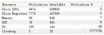
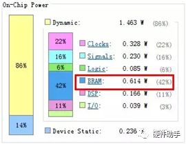
In the figure below, although BRAM is only used at 7%, its power consumption of 0.614W accounts for 42% of the total design, so optimizing BRAM power consumption can effectively reduce dynamic power consumption of the FPGA.
Below are methods to optimize BRAM power consumption:
-
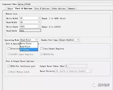
Use “NO CHANGE” mode: When configuring BRAM as True Dual Port, it is necessary to select the operation mode of the port: “Write First”, “Read First” or “NO CHANGE” to avoid conflicts between read and write operations, as shown in Figure 6; where “NO CHANGE” indicates that BRAM does not add extra logic to prevent read/write conflicts, thus reducing power consumption, but the designer must ensure that no read/write conflicts occur during program execution.
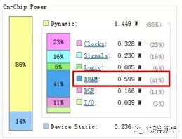
After setting to “NO CHANGE”, BRAM power consumption decreased from 0.614W to 0.599W. If a large amount of BRAM is used in the design, the effect will be even more pronounced.
-
Control the “EN” signal: There is a clock enable signal in the BRAM port, which can be enabled in the port settings, connecting it with read/write signals during module instantiation. This optimization can make BRAM stop working when there are no read/write operations, saving unnecessary power consumption.
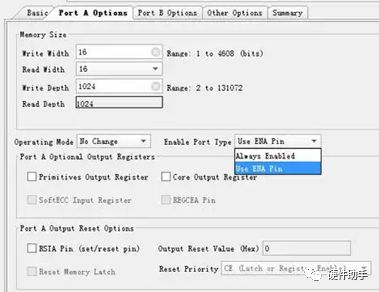
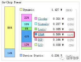
After optimizing the control of the “EN” signal, BRAM power consumption dropped to 0.589W.
-
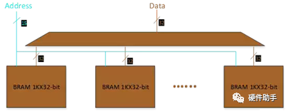
Depth Splicing: When a large amount of memory is used in the design, multiple blocks of BRAM need to be spliced together. For example, a depth of 32K and width of 32-bit requires a storage capacity of 32K*32Bit, but how to configure a single block of BRAM is an issue. In the 7 series FPGA, there is 36Kb of BRAM, where 32Kb capacity is generally used, so it can be configured as 32K*1-bit or 1K*32-bit. When splicing multiple blocks of BRAM, the former is “splicing width” and the latter is “splicing depth”. When working, the “splicing width” structure requires all BRAMs to perform read/write operations simultaneously, while the “splicing depth” structure only requires one block of BRAM to perform read/write, so when low power consumption is needed, the “splicing depth” structure should be adopted. However, it is important to note that the “splicing depth” structure requires additional data selection logic, increasing the logic levels, thus sacrificing both area and performance to reduce power consumption.
3. Power-Up and Power-Down Timing
3.1. Power-Up Timing
FPGA usually requires multiple power supply voltages and requires a specific power-up/power-down sequence. Sequential power-up helps limit inrush current during power-up. Ignoring the power supply sequence requirements of the device may lead to device damage or latch-up, causing FPGA device failure. There are three types of power-up timing: synchronous tracking, sequential tracking, and ratio tracking.
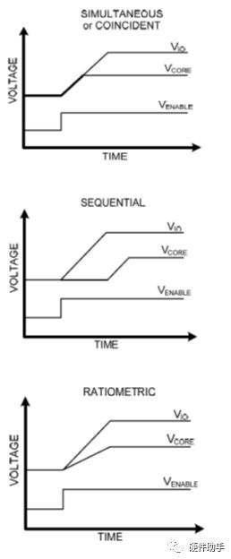
For various series of FPGA chips, the internal power-up timing of each functional module is generally independent, but there are specific requirements for the order of each functional module. Detailed information can be found in the data sheets of each device, which will specify detailed ordering constraints.
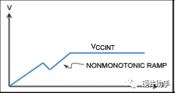
3.2. Monotonic Rise
It is very important to maintain a monotonic rise of the power supply voltage during startup to ensure that the device successfully powers on. General FPGA specifications provide strict requirements for voltage monotonic rise, meaning that the power supply voltage should continuously rise to the set regulated value without dropping in between. If the power supply cannot provide sufficient output power, it will result in a drop.
3.3. Power-On Time
Most FPGAs specify minimum and maximum values for the rise rate of the startup voltage, and the power supply achieves soft start by gradually increasing the current limit during startup. Soft start slows down the rise rate of the power supply voltage and reduces the peak inrush current injected into the FPGA. General power supplies can set soft start time using capacitors connected to the pins.
3.4. Power-Off Timing
Power-off timing also needs to be controlled, with the standard timing being the reverse of the power-up timing.
3.5. Timing Control for Special Cases
There are often cases where FPGA is interconnected with other CPUs such as ARM. To avoid damaging the device, the power-up timing of both FPGA and ARM must satisfy their respective power-up timing requirements. This situation can be handled as follows:
-
When FPGA and ARM each use their own configuration files: Since ARM is in a reset state, its IO is in input state, while FPGA needs to complete configuration before determining its IO state. Therefore, FPGA and ARM can perform their own power-up timing. When ARM’s power-up timing is completed, it remains in a reset state, so its IO is in input state. When FPGA completes power-up, it configures itself and sends a configuration completion signal to release ARM’s reset, setting the corresponding IO state, thus avoiding IO conflicts and not affecting the FPGA startup timing, preventing latch-up effects at the FPGA interface.
-
When FPGA is configured by ARM, there will be no IO conflict, since before FPGA releases its reset and begins configuration, its IO is in high impedance state, and the FPGA does not have a configuration file, so it will not set the IO state.
4. Power Supply Solutions
Currently, common power supply solutions for FPGA include using single LDO, single DC/DC, single Power Module, PMIC, etc.
4.1. LDO
If PCB space is guaranteed, low output noise is important, or if the system requires quick response to input and transient phenomena, LDO should be used. LDO provides medium to low output current. Input capacitance usually cuts the impedance and noise to the LDO. LDO also requires a capacitor at the output to handle system transient response and provide stability.
4.2. SMPS
When design efficiency is crucial and the system requires high output current, switch-mode power supplies have advantages. Switch-mode power supplies provide higher efficiency than LDO, but their switching characteristics make them more sensitive to noise. Unlike LDOs, switch-mode power supplies require inductors and may require transformers for DC-DC conversion, which demands more PCB space.
4.3. Power Module
Power Modules can eliminate the need to build peripheral circuits on your own, and modules designed by manufacturers generally perform better (higher efficiency, lower ripple) than self-designed solutions, but power modules are typically chosen in cases with high current demands.
4.4. PMIC
Due to the widespread application of FPGA, there are increasingly more dedicated PMICs for FPGA, which can meet the specific needs of certain FPGA chips in terms of output voltage, number of channels, output current, etc., while having advantages in PCB space usage, design convenience, and price. For the ZU+ MPSoC series, please refer to the previous article “Power Supply for Zynq UltraScale+ Series”, other series are similar. Detailed information can be found on the official websites of manufacturers like TI, Infineon, ADI (including Linear Technology), which provide corresponding solutions for FPGA series chips.
The above is an introduction to the power supply for Xilinx FPGA, mainly including types of power supply, voltage requirements, power consumption analysis, power-up and power-down timing, and power implementation methods.

Welcome FPGA, embedded, signal processing, and other engineers to follow our public account

The largest FPGA WeChat technical group in the country
Welcome everyone to join the national FPGA WeChat technical group, which has tens of thousands of engineers and a group of technology-loving engineers. FPGA engineers here help each other, share knowledge, and the technical atmosphere is strong! Hurry up and invite your friends to join!!

Press and hold to join the national FPGA technical group
FPGA Home Component City
Advantageous component services, please scan the code to contact the group owner: Jin Juan Email: [email protected] Welcome to recommend to procurement
ACTEL, AD part advantageous ordering (full series):
XILINX, ALTERA advantageous stock or ordering (full series):
(The above components are part of the models, for more models please consult group owner Jin Juan)
Service philosophy: FPGA Home Component self-operated city aims to facilitate engineers to quickly and conveniently purchase components. After years of sincere service, our customer service is spread across large listed companies, military research units, and small and medium-sized enterprises in China. Our greatest advantage is emphasizing the principle of service first and achieving fast delivery and favorable prices!
Directly operated brands: Xilinx, ALTERA, ADI, TI, NXP, ST, E2V, and over a hundred component brands, especially skilled in dealing with components subject to embargoes from the US and Europe,engineer friends are welcome to recommend us to procurement or consult us directly!We will continue to provide the best service in the industry!

FPGA technical group official thanks to brands: Xilinx, intel (Altera), microsemi (Actel), LattIC e, Vantis, Quicklogic, Lucent, etc.