With the rise of Internet of Things (IoT) technology, it has become increasingly common for electronic products to be equipped with wireless communication capabilities. Wireless communication technology relies on RF circuits on PCBs to achieve this. Unfortunately, even the most skilled PCB designers often shy away from RF circuit design due to the significant design challenges it presents, requiring specialized design and simulation analysis tools. As a result, for many years, the RF sections of PCBs have been designed by independent designers with RF design expertise.
RF circuit design engineers have employed various techniques, and after a vigorous effort, they have produced the RF circuit layout shown below, exporting it in DXF format for PCB layout to replicate. Isn’t that delightful? 

After importing the RF circuit DXF file, the PCB designer noticed that the traces had both right angles and sharp corners. They thought to themselves, “Hmm, this RF design is quite poor, and the salary is higher than mine. They don’t even understand how to avoid sharp corners and use rounded transitions,” and then they optimized the routing for the RF circuit section.
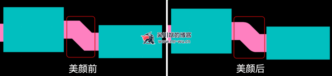
The result…
To avoid misunderstandings in the future, after work, the RF engineer called the layout engineer over, closed the door, and provided hands-on guidance on some key points of RF PCB design.

According to RF circuit theory, when the wavelength of the signal transmitted on the connection line is comparable to the geometric dimensions of discrete circuit components, the pads of RF IC pins, the transmission lines of RF signals on the PCB, RF passive components, vias, and even the copper pour for grounding are all critical factors that significantly affect the performance of RF signals.
Microstrip lines are an ideal choice for transmitting high-frequency signals on PCBs. Unless the connection distance between the IC and the antenna is very short, coaxial cables or transmission lines with characteristic impedance matching should be used. On printed circuit boards, it is best to use microstrip line structures as shown in the figure below.
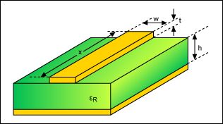
Microstrip line transmission lines consist of fixed-width metal traces (conductors) and a ground area directly below (in the adjacent layer). For example, the traces on layer 1 (top metal) require a solid ground area on layer 2. The width of the traces, the thickness of the dielectric layer, and the type of dielectric determine the characteristic impedance (typically 50Ω or 75Ω).
Of course, in addition to microstrip lines, another common transmission line is the stripline, as shown in the figure below.
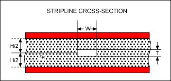
Stripline consists of fixed-width traces in the inner layer, with ground areas above and below. The conductor can be centered in the ground area or offset. This method is suitable for RF traces in inner layers.
Since striplines are also suitable for RF traces, why does the author say that microstrip lines are the ideal choice for transmitting high-frequency signals on PCBs?
Both microstrip lines and striplines perform excellently at millimeter-wave frequencies, but the difference lies in manufacturing costs.
Compared to stripline circuits, microstrip line circuits have fewer processing steps, and circuit components are easier to place, making them easier to manufacture (lower manufacturing costs).
In contrast to microstrip lines, striplines provide more isolation for adjacent electrical lines, supporting denser component layouts. Additionally, stripline circuits are very suitable for manufacturing multilayer PCBs, where each layer can be well isolated.
The electrical performance of both microstrip and stripline conductors is affected by the dielectric constant of the insulating material and the proximity effect of the ground layer. Microstrip lines have only one ground layer, while striplines have two. For microstrip lines, the effective dielectric constant affecting the conductor impedance is the sum of the relative dielectric constants of the insulating material and the air above the circuit (equal to 1). The effective dielectric constant for striplines is the sum of the relative dielectric constants of the two substrates above and below the conductor.
For all high-frequency circuits, maintaining controlled impedance is crucial for achieving consistent amplitude and phase response electrical performance. The impedance of the conductors in both types of transmission lines, among other factors, is a function of the conductor width, conductor thickness, thickness of the insulating substrate, and the relative permittivity or dielectric constant of the substrate. For striplines, it does not matter whether the distance between the center conductor and the two ground layers is equal, or whether the dielectric constants of the insulating materials above and below the conductor are the same (the same applies to microstrip lines).
Striplines have two ground layers, so a 50Ω (or any given impedance) stripline is thinner than a microstrip line with the same conductor impedance. Thinner lines support greater circuit density, but they also require stricter manufacturing tolerances, and the dielectric constant of the entire circuit substrate must be very consistent. The dielectric loss of a microstrip line’s single-ended (unbalanced) transmission line (defined by the dissipation factor of the substrate) is less than that of a stripline because some of the field lines of the microstrip line are in the air, where the dissipation factor is negligible.
Of course, the performance of both types of transmission lines is essentially similar to the performance of the substrate used for their manufacture—the insulating substrate. As with the PCB materials used, such as FR-4, which can reduce costs but also limit performance, selecting the most suitable materials for different microstrip and stripline applications will better leverage the advantages of these two transmission lines.
As with many engineering decisions, there is a trade-off in choosing between microstrip lines and striplines. For example, stripline circuits have higher circuit density, thus requiring more material layers, more processing time and costs, and greater attention to detail compared to microstrip line circuits under the same frequency conditions.
In addition to the common microstrip and stripline, another RF transmission line is the grounded coplanar waveguide, which provides better isolation between adjacent RF lines and other signal lines. This medium includes a central conductor and ground areas on both sides and below, as shown in the figure:
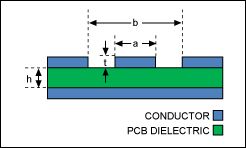
It is recommended to install via “fences” on both sides of the grounded coplanar waveguide, as shown in the figure. This top view provides an example of installing a row of ground vias in the top metal ground area on each side of the central conductor. The return current induced on the top layer is shorted to the ground layer below.
Compared to microstrip lines, the grounded coplanar waveguide has a larger grounding area because it has a ground plane not only on the bottom of the dielectric but also on both sides of the signal transmission line on the top of the dielectric. The coplanar waveguide achieves stable electrical performance by surrounding the signal line with ground planes.
The transmission modes of microstrip lines and grounded coplanar waveguide circuits are both quasi-transverse electromagnetic modes (quasi-TEM). Due to the enhanced grounding structure of the grounded coplanar waveguide circuit, its mechanical processing is also somewhat more complex. Compared to microstrip lines, grounded coplanar waveguide circuits have lower radiation loss characteristics, especially when the frequency rises to the millimeter-wave band.
Due to the enhanced grounding structure, grounded coplanar waveguide circuits have a wider effective bandwidth and a larger impedance range than microstrip line circuits. However, the microstrip line circuit structure is relatively robust, and its simple bottom ground plane circuit structure is easy to process. Additionally, the performance of microstrip line circuits is less sensitive to circuit processing factors, and their circuit performance is less affected by variations in conductor/spacing etching and conductor thickness.
As for the sharp corners in the RF circuit layout, they are intentionally designed for transmission line bend compensation.
When routing constraints require the transmission line to bend (change direction), the bending radius used should be at least three times the width of the central conductor. In other words:
Bending radius ≥ 3 × (line width).
This minimizes the change in characteristic impedance at the bend.
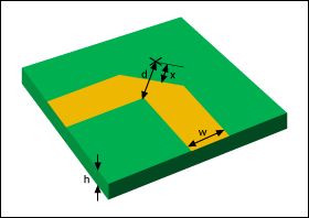
If gradual bending is not possible, the transmission line can be bent at right angles (non-curved), as shown in the figure. However, compensation must be made to reduce the impedance discontinuity caused by the increase in local effective line width at the bend point.