Welcome FPGA engineers to join the official WeChat technical group
Clickthe blue textto follow us at FPGA Home – the best pure engineer community in China
Detailed Explanation of Xilinx RapidIO Core
1. Overview of RapidIO Core
The design standard for the RapidIO core comes from the RapidIO Interconnect Specification rev2.2, which supports three modes: 1x, 2x, and 4x. Each channel supports speeds of 1.25Gbaud, 2.5Gbaud, 3.125Gbaud, 5.0Gbaud, and 6.25Gbaud.
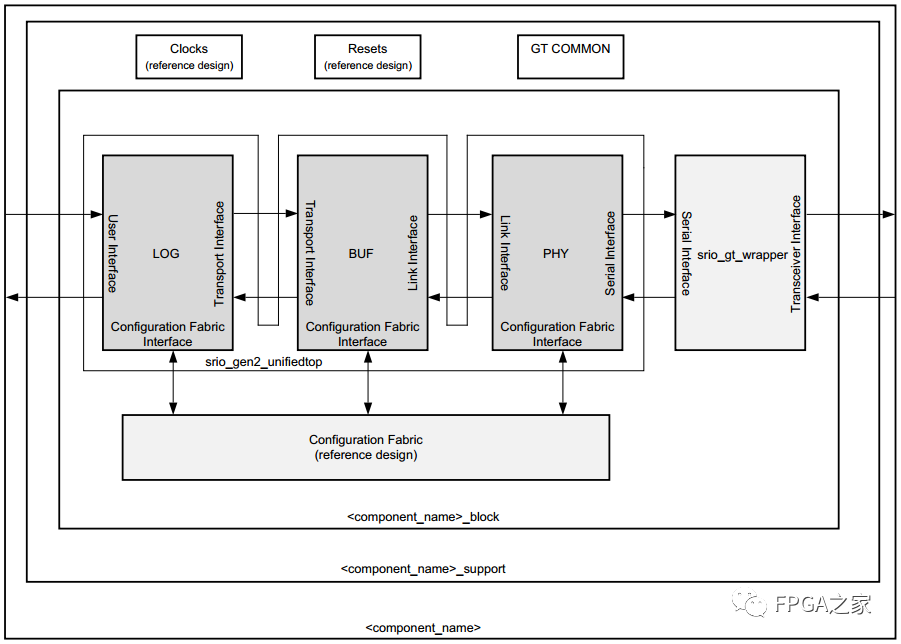
The RapidIO core is divided into three parts: Logical Layer, Buffer, and Physical Layer. The Logical Layer supports simultaneous operations by both the Initiator and Target; it supports Doorbell transactions and Message transactions, and has a dedicated port for Maintenance transactions; it uses AXI4-Lite and AXI4-Stream interfaces, supporting a simple handshake mechanism to control data flow; it supports programmable Source ID and 16-bit device IDs (optional). The Buffer layer supports independently configurable TX and RX Buffer depths of 8, 16, and 32 packets; it supports independent clocks and optional flow control for sending data. The Physical Layer supports configurable Idle Sequence 1 and Idle Sequence 2; it supports Critical Request Flow; and it supports multicast events.
Note: Explanations for the above professional terms can be found in previous blogs. If you are unclear, you can refer back to them.
The RapidIO interconnect architecture is compatible with most popular integrated communication processors, host processors, and network digital signal processors. It is a high-performance, packet-switched interconnect technology that meets the demands for reliability, increased bandwidth, and faster bus speeds in high-performance embedded industrial systems.
The RapidIO standard is defined in three layers: the Logical Layer, the Transport Layer, and the Physical Layer. The Logical Layer defines the overall protocol and packet format. It includes the necessary information for RapidIO devices to initiate and complete transactions. The Transport Layer provides routing information during the transmission of RapidIO packets. The Physical Layer describes device-level interface details such as packet transmission mechanisms, flow control, electrical characteristics, and low-level error management. This division allows for flexible addition of new transaction types to the Logical Layer specification without modifying the Transport or Physical Layer specifications.
The architecture of the entire RapidIO core is shown in the figure below:
2. RapidIO Core Interface Description
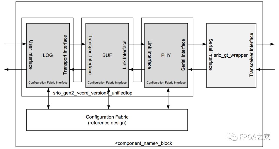
The RapidIO core encapsulates three sub-cores, providing a high-level, low-maintenance interface. This section introduces the basic functional view of each sub-core and interface of RapidIO. The top-level block diagram of the RapidIO core is shown in the figure below:
2.1 Logical Layer Interface
The Logical Layer (LOG) is divided into several modules to control and parse sent and received data packets. The Logical Layer has three interfaces: User Interface, Transport Interface, and Configuration Fabric Interface.
The following diagram shows the logical interface:
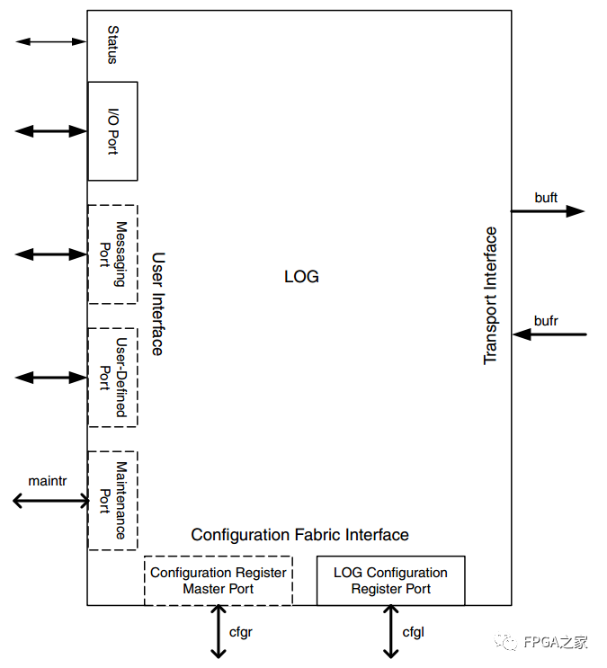
The User Interface includes ports that can initiate and receive packets. When generating the IP core, the number of ports and transaction types can be configured, and maintenance transactions can be initiated to access and configure local or remote registers via the AXI4-Lite interface.
The Transport Interface consists of two ports for sending and receiving, which connect to the intermediate Buffer. For the top-level module of RapidIO, these two interfaces are invisible.
The Configuration Interface also includes two ports. The Configuration Master Port is used to read and write the local configuration space. The LOG Configuration Register Port can be used to read and write some configuration registers of the Logical Layer or Transport Layer.
The most important aspect for users of the RapidIO IP core is the User Interface, which is detailed below.
The User Interface includes a set of I/O ports and three optional ports: the Messaging Port, the Maintenance Port, and the User-Defined Port. These interfaces are at the top level of the module, and each transaction type is transmitted on designated ports. Among them, all supported I/O transactions, such as NWRITEs, NWRITE_Rs, SWRITEs, NREADs, and RESPONSEs (excluding responses for maintenance transactions), are sent or received on the I/O ports. Message transactions can be transmitted on the I/O port or the Messaging Port, depending on whether the I/O port and Message port are separated in the configuration of the IP core. Doorbell transactions can only be transmitted on the I/O port and not on the Messaging Port. Maintenance transaction packets can only be transmitted on the Maintenance Port. If the transaction is a user-defined unsupported type, it can be transmitted on the User-Defined Port; if the User-Defined Port is not enabled in the IP core configuration, the user-defined packet will be discarded.
The I/O Port
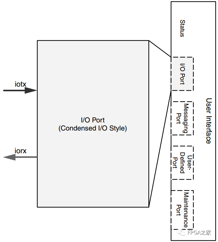
The I/O port can be configured as two types: Condensed I/O or Initiator/Target. These two types can be selected in the configuration of the IP core. The data flow protocol for the I/O port is the AXI4-Stream protocol, which supports two types of packet formats: HELLO format and SRIO Stream format.
The Condensed I/O port type reduces the number of ports used for sending and receiving I/O packets. It uses only one AXI4-Stream channel to send all types of packets, and similarly, it uses only one AXI4-Stream channel to receive all types of packets. The schematic diagram of the Condensed I/O port is shown below:
The Initiator/Target port type processes request transactions and response transactions separately, so there are a total of four AXI4-Stream channels for transmitting I/O transactions. The schematic diagram of the Initiator/Target port is shown below, where the gray arrows indicate request transactions, and the black arrows indicate response transactions.
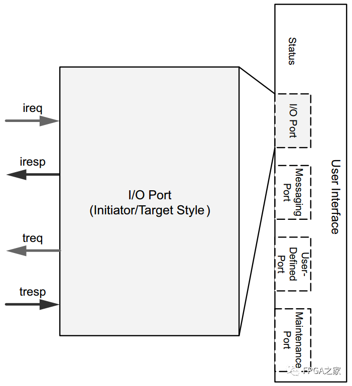
Requests generated by the local device are sent through the ireq channel, while response packets generated by the remote device are received through the iresp channel to complete the entire transaction interaction process.
Requests generated by the remote device are received through the treq channel, while response packets generated by the local device are sent through the tresp channel to complete the entire transaction interaction process.
In the top-level module, the variable names correspond to the channels as follows:
s_axis_ireq* corresponds to the ireq channel
m_axis_iresp* corresponds to the iresp channel
m_axis_treq* corresponds to the treq channel
s_axis_tresp* corresponds to the tresp channel
Messaging Port
The Messaging Port is an optional interface where message transactions can be sent either on the I/O port or on the independent Messaging Port. The independent Messaging Port type is Initiator/Target type. The diagram of the Messaging Port is shown below:
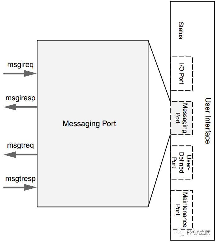
Requests generated by the local device are sent through the msgireq channel, while response packets generated by the remote device are received through the msgiresp channel to complete the entire transaction interaction process.
Requests generated by the remote device are received through the msgtreq channel, while response packets generated by the local device are sent through the msgtresp channel to complete the entire transaction interaction process.
In the top-level module, the variable names correspond to the channels as follows:
s_axis_msgireq* corresponds to the msgireq channel
m_axis_msgiresp* corresponds to the msgiresp channel
m_axis_msgtreq* corresponds to the msgtreq channel
s_axis_msgtresp* corresponds to the msgtresp channel
User-Defined Port
The User-Defined Port is an optional port that includes two AXI4-Stream channels, one for sending and the other for receiving. The User-Defined Port only supports SRIO Stream format transactions. The diagram of the User-Defined Port is shown below:
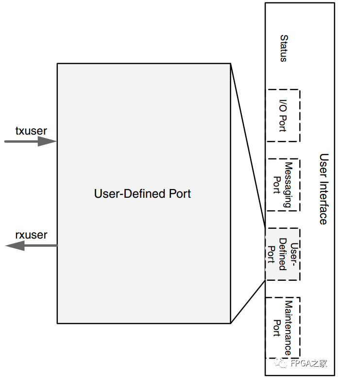
In the top-level module, the variable names correspond to the interfaces as follows:
s_axis_usrtx* corresponds to the user_io_tx interface
m_axis_usrrx* corresponds to the user_io_rx interface
Maintenance Port
The Maintenance Port uses the AXI4-Lite interface protocol, allowing users to access local or remote configuration spaces. The diagram of the AXI4-Lite maintenance port is shown below:
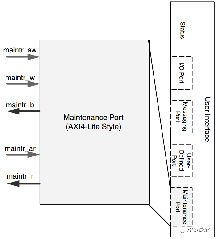
The black arrows from right to left in the figure indicate request channels, while the gray arrows from left to right indicate response channels. Each channel has independent ready/valid handshake signals.
Status
The status signals for the user interface include deviceid and port_decode_error, defined in the table below:
|
Signal |
Direction |
Description |
|
deviceid[15:0] |
Output |
Value of the Base DeviceID CSR (offset address 0x60) register |
|
port_decode_error |
Output |
This signal is high when the user-defined port is not enabled, indicating that an unsupported transaction has been received and will be immediately discarded. This signal goes low after the next supported transaction packet is received on any user interface. This signal is synchronized with the log_clk signal |
2.2 Buffer Interface
The purpose of the Buffer is to buffer the packets sent and received. Buffering is essential for ensuring packet transmission and flow control operations. Xilinx provides a configurable Buffer solution that allows for a trade-off between system performance and resource utilization.
The sending Buffer is responsible for queuing transactions that are about to be sent and managing the packet flow to the Physical Layer (PHY). The sizes of the receiving Buffer and sending Buffer can be configured in the IP core to depths of 8, 16, or 32 packets. The sending Buffer is a store-and-forward buffer that is used to minimize packet-to-packet latency to maximize flow throughput. The sending Buffer must hold each packet until it is successfully received by the recipient; only after successful reception will the sending Buffer release the packet to make space for other packets. During flow control events, multiple unsent packets may remain in the sending Buffer, which will reorder the sending Buffer based on the type and priority of packets, sending response packets first and request packets afterwards.
The Buffer’s other function is to handle cross-clock domain issues. When generating the IP core, cross-clock domain logic can be added or removed as needed. For multi-channel RapidIO, since the clock at the Physical Layer is dynamic in start-up and traindown scenarios, it is recommended to add cross-clock domain logic to ensure user logic operates at known rates.
The receiving Buffer is similar to a FIFO, used to store and forward data sent to the Logical Layer on the receiving path. The receiving Buffer also includes cross-clock domain logic, ensuring that the Logical Layer and Physical Layer work at different rates. Like the sending Buffer, it is recommended to add cross-clock domain logic for multi-channel RapidIO.
All Buffer layer interfaces are invisible to the top level of RapidIO. The schematic diagram of the Buffer layer is shown below:
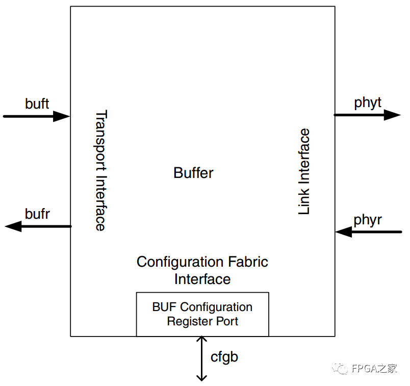
As can be seen from the above diagram, there are two AXI4-Stream channels on both sides of the Logical Layer and Physical Layer in the Buffer layer, one for sending and the other for receiving. There is also an AXI4-Lite channel used to configure the Buffer layer’s configuration space.
2.3 Physical Layer Interface
The Physical Layer (PHY) handles link training, initialization, and protocol, as well as the insertion of packet cyclic redundancy check (CRC) and acknowledgment identifiers. The physical layer interface connects to high-speed serial transceivers. The serial transceiver is designed as an external instantiated module in the IP core to reduce the difficulty of user model usage. The schematic diagram of the physical layer interface is shown below:
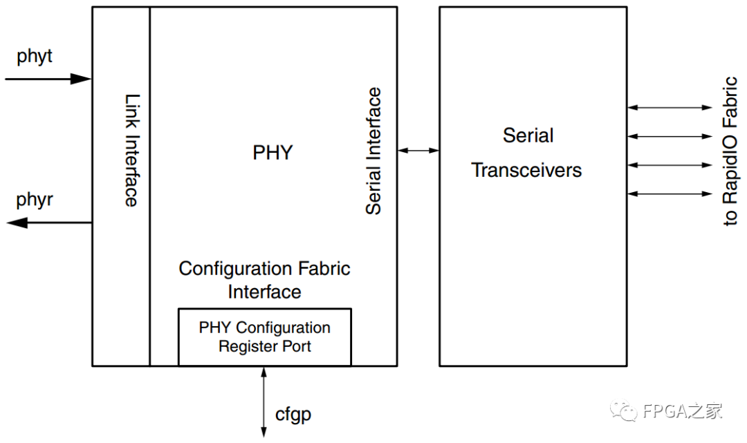
The Physical Layer is connected to the Buffer Layer via two AXI4-Stream channels, while the Physical Layer has one AXI4-Lite interface channel connected to the configuration structure, allowing access to the Physical Layer’s configuration space. The Physical Layer also connects to the serial transceivers via a serial interface.
2.4 Register Space
The register space of RapidIO is shown in the table below:
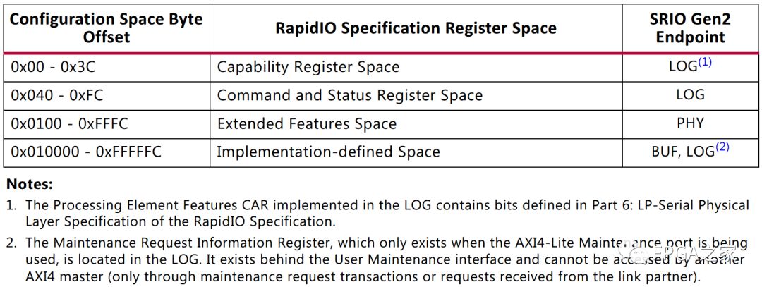
Capability Register Space
The registers in the Capability Register Space are read-only registers implemented in the Logical Layer. The mapping table for the capability registers is shown in the table below:
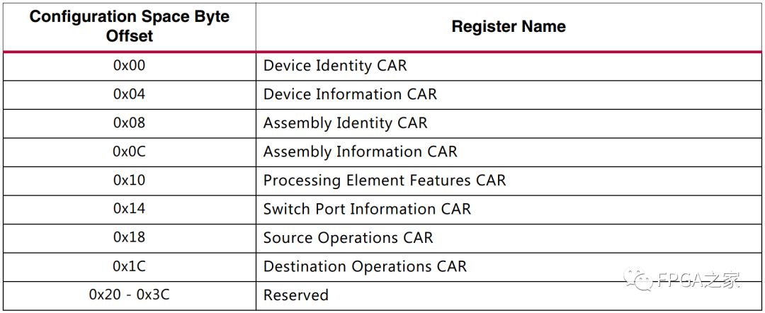
Command and Status Register Space
The registers in the Command and Status Register Space, like the capability registers, are implemented in the Logical Layer. The mapping table for the Command and Status Register Space is shown in the table below:
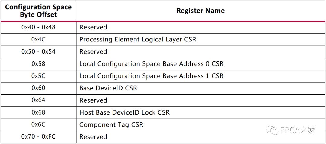
The register space also includes Extended Feature Space and Implementation-defined Space. For explanations about these two types of register spaces, please refer to pg007_srio_gen2.pdf.
3. Using the RapidIO Core
3.1 Design Guidelines
The RapidIO protocol defines seven types of transactions, each performing different functions. The FTYPE and TTYPE fields in the RapidIO packet format together determine the transaction type. Unlike the standard RapidIO protocol, the RapidIO core defines the 9th type of transaction (FTYPE=9) – DATA STREAMING transaction, which is a write transaction with a data payload, while the 9th type in the standard RapidIO protocol is a reserved transaction. The detailed correspondence is shown in the table below:
|
Ftype (Format Type) |
Ttype (Transaction Type) |
Packet Type |
Function |
|
0~1 |
—— |
Reserve |
None |
|
2 |
4’b0100 |
NREAD |
Read from specified address |
|
4’b1100 |
ATOMIC increment |
First pass data to the specified address, then increment the data; this operation is atomic and cannot be interrupted |
|
|
4’b1101 |
ATOMIC decrement |
First pass data to the specified address, then decrement the data; this operation is atomic and cannot be interrupted |
|
|
4’b1110 |
ATOMIC set |
Set all bits of the data at the specified address to 1 |
|
|
4’b1111 |
ATOMIC clear |
Clear the data at the specified address (set all bits to zero) |
|
|
3~4 |
—— |
Reserve |
None |
|
5 |
4’b0100 |
NWRITE |
Write data to the specified address |
|
4’b0101 |
NWRITE_R |
Write data to the specified address and receive the response from the target device after writing |
|
|
4’b1101 |
ATOMIC test/swap |
Test and swap the data at the specified address; this operation is atomic and cannot be interrupted |
|
|
6 |
4’bxxxx |
SWRITE |
Write to the specified address in stream mode; this method is the most efficient compared to NWRITE and NWRITE_R |
|
7 |
—— |
Reserve |
None |
|
8 |
4’b0000 |
MAINTENANCE read request |
Initiate read configuration, control, and status register request |
|
4’b0001 |
MAINTENANCE write request |
Initiate write configuration, control, and status register request |
|
|
4’b0010 |
MAINTENANCE read response |
Generate read configuration, control, and status register response |
|
|
4’b0011 |
MAINTENANCE write response |
Generate write configuration, control, and status register response |
|
|
4’b0100 |
MAINTENANCE write request |
Port write request |
|
|
9 |
—— |
DATA Streaming |
Data stream write; request transaction contains valid data |
|
10 |
4’bxxxx |
DOORBELL |
Doorbell |
|
11 |
4’bxxxx |
MESSAGE |
Message |
|
12 |
—— |
Reserve |
None |
|
13 |
4’b0000 |
RESPONSE no data |
Response packet without valid data |
|
4’b1000 |
RESPONSE with data |
Response packet with valid data |
|
|
14~15 |
—— |
Reserve |
None |
Logical Layer AXI4-Stream Serial RapidIO Interface Usage
The transaction sending and receiving interface of the RapidIO core adopts the AXI4-Stream protocol. The AXI4-Stream protocol uses ready/valid handshake signals to transmit information between master and slave devices. The AXI4-Stream protocol uses the tlast signal to indicate the last data of the transmission to determine the packet boundary and uses the tkeep byte enable signal to indicate valid bytes in the data. It also includes valid data tdata signals and user data tuser signals for transmitting actual packet data.
HELLO Packet Format (Key Point)
To simplify the construction process of RapidIO packets, the transaction transmission interface (ireq, treq, iresp, tresp) of the RapidIO core can be configured to HELLO (Header Encoded Logical Layer Optimized) format. This format standardizes the header domain of the packet and separates the header and data for transmission on the interface, simplifying control logic and allowing data to align with the sending boundary, which helps with data management.
The HELLO format packet is shown in the figure below:
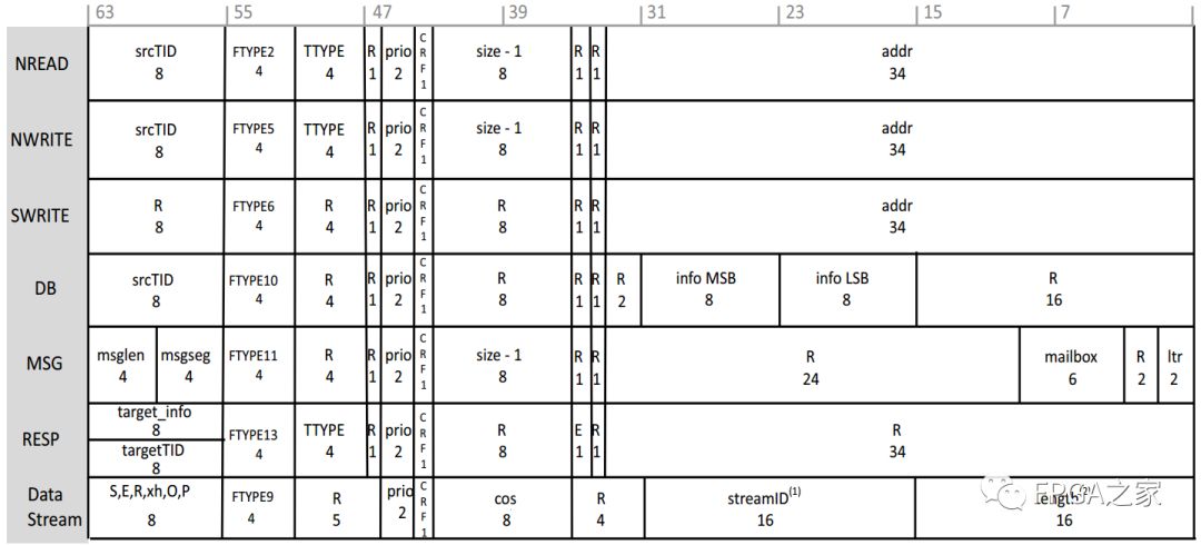
Where the definitions of each field are shown in the table below:
|
Field |
Position |
Description |
|
TID |
[63:56] |
Transaction ID of the packet; according to the RapidIO manual, at any given time, a RapidIO packet can only have a unique TID associated with the Src ID. |
|
FTYPE |
[55:52] |
Transaction class of the packet; the supported FTYPEs for HELLO format are 2, 5, 6, A, B, and D. |
|
TTYPE |
[51:48] |
Transaction type of the packet; when the value of FTYPE is 2, 5, or D, different TTYPE values correspond to different functions of the packet. |
|
Priority |
[46:45] |
Priority of the packet; the priority value of request packets is 0~2, while the priority value of response packets is one more than the request packet’s priority. |
|
CRF |
[44] |
Critical Request Flow flag of the packet. |
|
Size |
[43:36] |
Number of valid data payload bytes minus 1; if this field’s value is 0xFF, it indicates that the valid data is 256 (0xFF + 1) bytes. |
|
Error |
[35] |
This field indicates an error state when it is set to 1. |
|
Address |
[33:0] |
Byte address of the transaction. |
|
Info |
[31:16] |
Information field; this field is included only in Doorbell transactions. |
|
Msglen-1 |
[63:60] |
Number of packets in the message transaction; this field is included only in Message transactions. |
|
Msgseg-1 |
[59:56] |
Message segments in the packet; this field is included only in Message transactions; if it is a single-segment message, this field is reserved. |
|
Mailbox |
[9:4] |
Destination mailbox of the packet; this field is included only in Message transactions; except for single-segment messages, the high four bits of this field are reserved. |
|
Letter |
[1:0] |
Letter of the packet; this field is included only in Message transactions, indicating a slot in the mailbox. |
|
S,E,R,xh,O,P |
[63:56] |
S: Start bit; when this field is 1, it indicates that this packet is the first segment of a new PDU (Protocol Data Unit). E: End bit; when this field is 1, it indicates that this packet is the last segment of a new PDU. When both S and E are 1, it indicates that the PDU contains only one packet. R: Reserved bit. Xh: Extended header; not supported in the current version. O: Odd; when this field is 1, it indicates that the data payload has an odd number of half-words. P: Padding bit; when this field is 1, a padding byte is used to pad data to half-word boundaries. |
|
Cos |
[43:36] |
Class of service. |
|
StreamID |
[31:16] |
Point-to-point data stream identifier. |
|
Length |
[15:0] |
Length of the Protocol Data Unit (PDU). |
The value of the Size field in the HELLO format packet is equal to the total number of bytes transmitted minus 1. The valid range for the Size field is 0~255, corresponding to actual transmitted byte counts of 1~256. The values of the size and address fields in the HELLO format must correspond to valid size, address, and wdptr values in the RapidIO packet, so there are some constraints on the values of the size and address fields in the HELLO format. The RapidIO core cannot correct illegal values in the Size field to valid values in the actual RapidIO packet’s Size field, so a correct value must be provided for the Size field in the HELLO format packet. Since the tdata signal in the AXI4-Stream protocol is 8 bytes, or one double word (Double Word), the value of the Size field needs to be discussed in two scenarios: when the amount of data transmitted is less than 8 bytes and when the amount of data transmitted is greater than 8 bytes.
When the amount of data transmitted is less than 8 bytes (Sub-DWORD Accesses):
For the case where the amount of data transmitted is less than 8 bytes, the address and size fields are used to determine the valid byte positions (the tkeep signal must be 0xff), but only combinations of address and size values that lead to valid values for rdsize/wrsize and wdptr in the RapidIO packet are allowed. The figure below shows the correspondence between the address and size fields in the HELLO format and the valid byte positions (the gray area in the figure indicates valid byte positions):
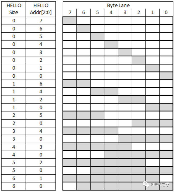
For example, for the combination of size=2 and address=34’h1_1234_5675, since size=2, the number of bytes written to the address is 3 (size+1), and the lowest 3 bits of the address are 5 (3’b101). According to the above figure, the valid byte positions are the 7th, 6th, and 5th bytes. Combinations of size and address[2:0] values that are not shown in the above figure are illegal and should be avoided, such as size=2 and address=34’h1_1234_5673, which is an illegal combination.
When the amount of data transmitted is greater than 8 bytes (Large Accesses):
For cases where the amount of data transmitted is greater than 8 bytes and the starting byte offset of the address is not 0, the data must be divided into multiple transmissions, and the unaligned segments of less than 8 bytes can be determined by the valid combinations of size and address shown in the above figure. Another solution is that the size of data for read operations can be increased to the next supported size, and then the necessary data can be extracted from the corresponding response.
Therefore, for a data amount of one double word (8 bytes) or larger, the lowest 3 bits of the address must be 0. The RapidIO manual defines the range of supported data amounts for read and write transactions from 1 to 256 bytes. If the data amount for request transactions exceeds one double word (8 bytes), the data amount should be rounded to the nearest supported value. The valid data amounts for HELLO format read and write transactions are: 7, 15, 31, 63, 95 (only supports read transactions), 127, 159 (only supports read transactions), 191 (only supports read transactions), 223 (only supports read transactions), and 255.
For write transactions with data amounts between the supported values mentioned above, the necessary data must be provided to the RapidIO core before the tlast signal of the channel is set to 1; only the provided data will be sent. Similarly, if the data provided by the user’s design is less than the expected data amount, the actual data amount should be written, and the transmission should be assumed to be complete.
The RapidIO protocol does not support transmitting data amounts greater than 256 bytes, and the Logical Layer cannot split data amounts greater than 256 bytes into smaller data amounts for sending. Failing to meet this requirement may lead to fatal link errors, in which case the link may continuously retransmit packets larger than 256 bytes.
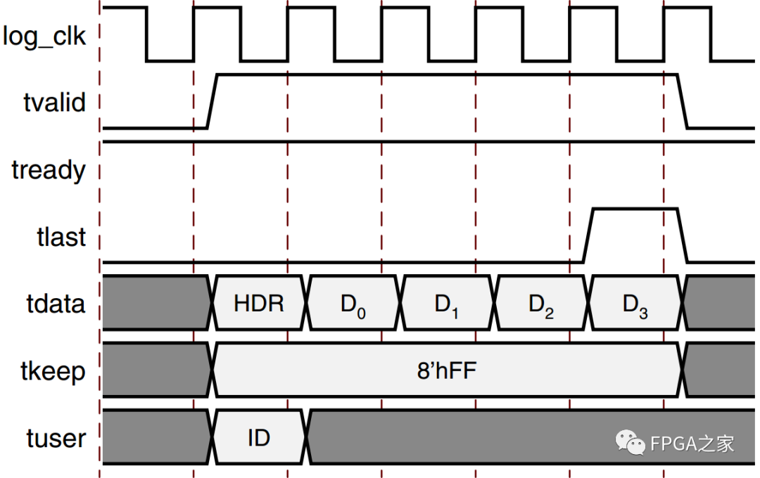
The header of the HELLO format data packet is transmitted on the first valid clock of the user interface. If the transmitted transaction carries a data payload, the data payload is sent immediately following the header, sequentially. The Source ID and Destination ID of the packet are sent in the tuser signal and are sent on the first valid clock just like the header; once sent, the data in the tuser signal is ignored.
The figure below shows the timing diagram of a HELLO format packet carrying a data payload transmitted on the user interface. This transmission has a data payload of 4 double words (32 bytes), and the entire transmission takes 5 clock cycles. The user only needs to send the data they want to send into the AXI4-Stream interface of the RapidIO core according to the timing diagram, and the RapidIO core will automatically convert it into a standard RapidIO serial physical layer packet for sending to complete a transaction interaction.
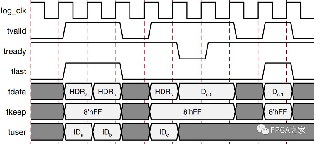
The figure below shows a more complex transmission diagram. First, there are two back-to-back single-cycle packets (packets without data payload, containing only a packet header). The packet boundary is indicated by raising the tlast signal. After the single-cycle packet transmission is completed, the master waits one clock cycle before starting to send the next packet. During the transmission of the third packet, the master (Master) and slave (Slave) each pause data transmission for one clock cycle by lowering the tvalid and tready signals. Since the data payload of the third packet is 2 double words, the total time consumed for transmitting the third packet is 3 valid clocks, plus 2 invalid clock cycles, resulting in a total of 5 clock cycles.
FPGA engineers and communication engineers are welcome to follow our public account
FPGA WeChat technical group
Welcome everyone to join the national FPGA WeChat technical group, where there is a group of engineers who love technology, and we can discuss technology together!
Press and hold to join the national FPGA technical group!
FPGA IP core services: various high-quality IP core service providers, with guaranteed service! If you have needs, you can contact the group owner directly!
The FPGA technical group platform operates: Xilinx Altera Micron, Samsung, Hynix, ADI TI ST NXP and other brand advantageous agents and distributors. If you have needs, please feel free to send the model list, and we will provide you with the most competitive quotes as soon as possible! Prices are more than 5% lower than your original supplier! Welcome to inquire – just send your needs to the group owner! We also hope you can recommend our WeChat to purchasing personnel. Thank you for supporting the pure technology platform, so we can do better and better —
Official thanks to the brands of the FPGA technical group: Xilinx, intel (Altera), microsemi (Actel), LattICE, Vantis, Quicklogic, Lucent, etc.