Welcome FPGA engineers to join the official WeChat technical group.
Clickthe blue textto follow us at FPGA Home – the largest pure engineer community for FPGA in China.
Xilinx-7 Series FPGA —-> Spartan-7 —-> General Logic
—-> Low-cost / Low-power
—-> High I/O performance
—-> Small package
—-> Artix-7 —-> Added PCIE interface
—-> Added Gigabit transceiver interface
—-> Larger logic density
—-> Kintex-7 —-> PCIE interface
—-> DSP Slices upgraded to DSP48 Slices
—-> GTP upgraded to GTX, faster rate
—-> Larger logic density
—-> Virtex-7 —-> Enhanced PCIE functionality
—-> Enhanced GTP functionality
—-> Larger logic density
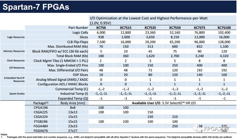
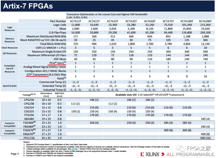
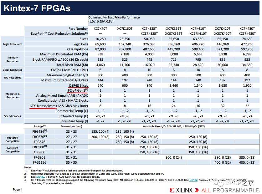
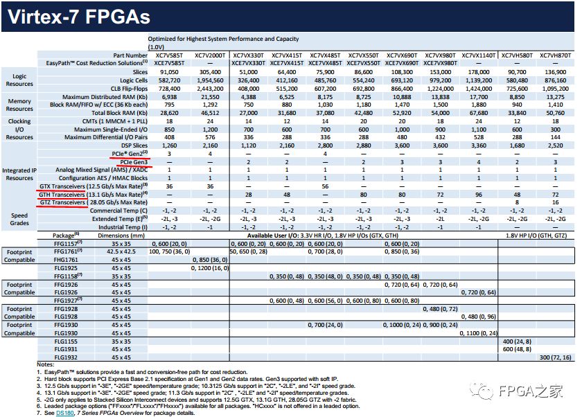
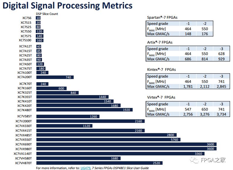
Comparison of DSP numbers:
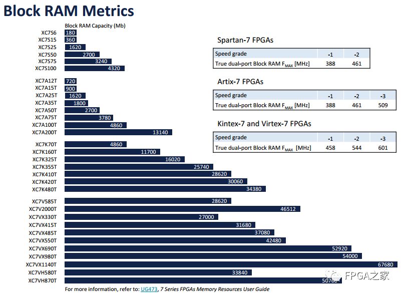
Comparison of BRAM numbers:
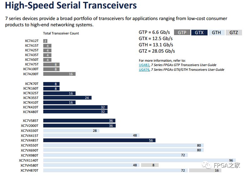
Comparison of high-speed serial transceivers:
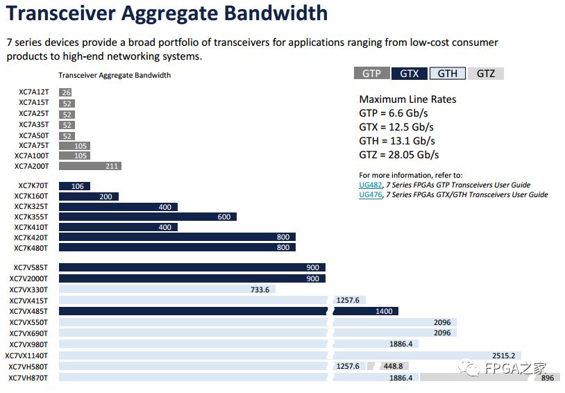
Comparison of total bandwidth of high-speed serial transceivers:
Comparison of I/O numbers and bandwidth:
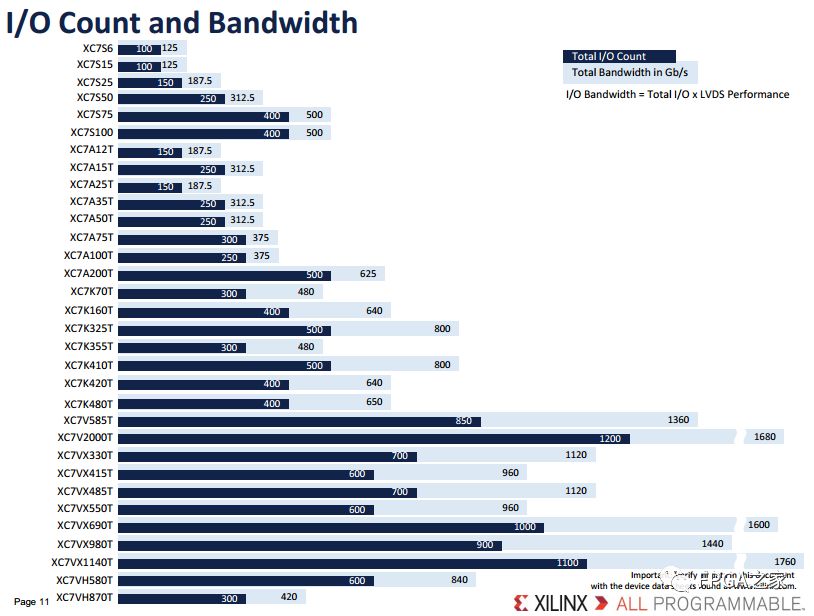
Xilinx 7-Series features —-> 28nm process
—-> I/O bandwidth: 2.9Tb/s
—-> Logic Cell capacity: 2,000,000
—-> DSP computation speed: 5.3TMAC/s
—-> Low power consumption
—-> True 6-input LUT, usable for distributed storage
—-> 36Kb dual-port BRAM, embedded FIFO logic, and on-chip data buffering
—-> SelectI/O technology supports DDR3 interface, speeds up to 1866Mb/s
—-> High-speed serial connections, speeds from 6.6Gb/s to 28.05Gb/s, supports low-power mode, optimized chip-to-chip interface
—-> User-configurable analog interface, dual 12-bit 1 MSPS (Million Samples per Second), on-chip temperature/power supply sensor
—-> DSP slices —-> 25×18 multipliers
—-> 48-bit accumulators
—-> High-performance filters
—-> Optimized equalizer filter
—-> CMT —-> PLL
—-> MMCM (Mixed-Mode Clock Management)
—-> MicroBlaze CPU —-> Integer computing capability 260 DMIPs ~ 441 DMIPs
—-> Integrated PCIe, x4 Gen2 ~ x8 Gen3, suitable for PCIe endpoint/root port design
—-> Memory 256-bit AES encryption, HMAC/SHA-256 verification, embedded SEU detection and error checking
—-> Environmentally friendly high performance
—-> 1.0V/0.9V core voltage
The following table more intuitively shows the differences between the categories:
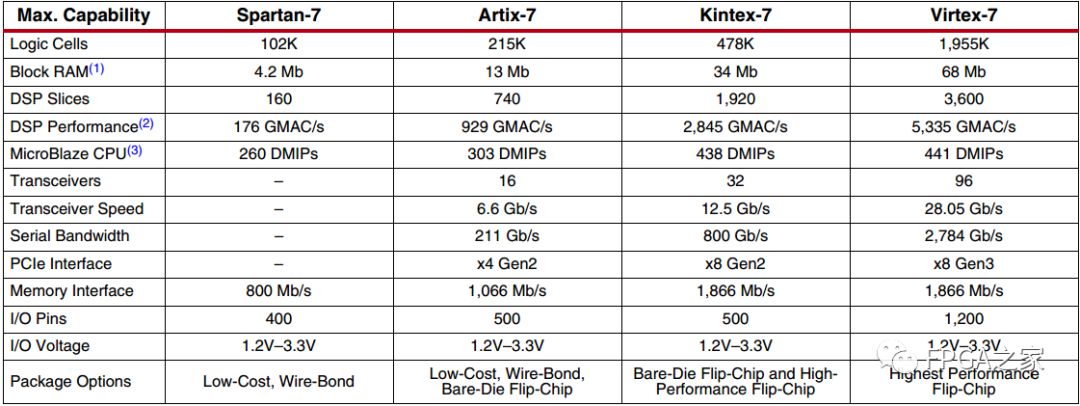
Some concepts:
—-> SSI technology —-> Uses multiple super logic domains SLR —-> Super high bandwidth connectivity
—-> Low latency
—-> Low power consumption
—-> Two types —-> Logic enhanced —-> Virtex-7T
—-> DSP/BRAM/transceiver dense —-> Virtex-7XT/HT
—-> High capacity/high performance/short cycle/low risk
—-> Super long wiring resources/super high-performance clock lines
—-> CLBs —-> True 6-input LUT —-> Can be configured as a 6-input single-output LUT/64-bit ROM
—-> 2 5-input LUTs/32-bit ROMs —-> each with one output
—-> Common address and logic inputs
—-> Each LUT output can optionally connect to a flip-flop
—-> 4 LUTs + 8 flip-flops + multiplexers + arithmetic carry logic —-> Slice
—-> 2 Slices —-> CLB
—-> 4 of the 8 flip-flops (one from each LUT in each Slice) —-> Latch
—-> LUT can be used as memory —-> 25% ~ 50% of all slices use their LUTs as 64-bit distributed RAM
—-> LUT can be used as registers and shift registers —-> 25% ~ 50% of all slices use their LUTs as 32-bit shift registers SRL32 or 2 SRL16
—-> Clock management —-> High-speed buffering and wiring
—-> Low jitter
—-> Frequency synthesis and phase shift
—-> Low jitter clock generator
—-> Filtering
—-> Up to 24 clock management channels CMTs —-> MMCM —-> Fractional counter
—-> Fixed or dynamic phase shift
—-> PLL
—-> Frequency synthesizer
—-> Clock jitter filtering
—-> Central VCO —-> Frequency size and PFD voltage to VCO
—-> 3 programmable frequency dividers —-> D —-> Input pre-divider
—-> M —-> Feedback divider
—-> O —-> Output divider
—-> 3 input jitter filtering options —-> Low bandwidth —-> Best jitter attenuation
—-> High bandwidth —-> Best phase offset
—-> Optimized mode —-> Balanced both
—-> Clock distribution —-> 6 different clock lines —-> BUFG/BUFR/BUFIO/BUFH/BUFMR/high-performance clock
—-> Global clock —-> 32 global clocks
—-> Can serve as clock for all flip-flops
—-> With enable/set/reset
—-> 12 clock lines driven by BUGH, can drive in any clock domain
—-> Each BUFH can independently enable control, so can turn off the clock in a domain
—-> Can be driven by global clock buffer —-> Faultless clock distribution and global clock enable
—-> Driven by CMT —-> Eliminates clock distribution delay
—-> Domain clock —-> Drives all clock targets within the domain
—-> Domain definition refers to the range of 50 I/O and 50 CLB and half-chip width
—-> 7 Series can have 2 ~ 24 domains
—-> Each domain has 4 domain clock paths
—-> Domain clock buffer driven by 4 clock input pins, can perform 1 ~ 8 division
—-> I/O clock —-> Fast
—-> Serves as I/O logic or serialization/deserialization circuit
—-> I/O can connect directly to MMCM
—-> Block RAM —-> Dual-port, 72-bit, 36kb BRAM
—-> Programmable FIFO logic
—-> Error checking circuit
—-> 5 to 1880 units
—-> Read and write synchronous operations
—-> Programmable data bit width
—-> DSP Slice —-> 25 × 18 dual-complement multiplier 48-bit high-resolution single multiplier
—-> Single Instruction Multiple Data (SIMD) unit/2 operands 10 different logic functions logic unit
—-> Low-power pre-accumulator
—-> Equalizer filter
—-> Pipelined/ALU/special bus cascading
—-> up to 741MHz
—-> 48-bit pattern detector
—-> High speed/high efficiency
—-> Dynamic bus converter
—-> Memory address generator
—-> Bus multiplexer
—-> I/O port memory-mapped registers
—-> Accumulator can be used as synchronous add/subtract counter
—-> Input/output —-> SelectIO technology
—-> 1,866Mb/s DDR3 interface
—-> On-chip high-frequency decoupling capacitors enhance signal integrity
—-> Supports various I/O standards
—-> HR IO —-> Wide voltage range (1.2V ~ 3.3V)
—-> HP IO —-> High-performance operation
—-> Organized by Bank, each Bank 50 pins
—-> Each Bank powered by VCCO
—-> Some single-ended input buffers require external reference voltage VREF
—-> Each Bank has 2 VREF pins (except for configuring Bank 0) —-> Only one VREF voltage value allowed
—-> Various packages
—-> Electrical characteristics —-> Pull-up and pull-down output structure
—-> Can be set to high impedance state
—-> Can set slew rate and output strength
—-> Can set pull-up and pull-down resistors
—-> Pin pairs can be set as differential input/output
—-> Can set 100-ohm internal termination resistor
—-> Various differential interface standards: LVDS, RSDS, BLVDS, differential SSTL, differential HSTL
—-> Each IO port supports memory interface standards
—-> T_DCI can control output drive impedance —-> Series termination/parallel shorting
—-> Saves PCB space
—-> Output mode or tri-state mode termination will automatically shut off
—-> IBUF and IDELAY have low power modes
—-> 8-bit IOSERDES can complete serialization and deserialization —-> Programmable width 2 to 8 bits
—-> Supports adjacent pin cascading
—-> Dedicated oversampling mode for data recovery —-> e.g., SGMII interface
—-> Low-power gigabit transceivers
—-> Integrated PCIe interface
—-> Configuration
—-> Analog-to-digital conversion

Welcome communication engineers and FPGA engineers to follow our public account.

National First FPGA WeChat Technical Group
Welcome everyone to join the national FPGA WeChat technical group, this community has tens of thousands of engineers, a group of engineers who love technology, where FPGA engineers help each other, share with each other, and have a strong technical atmosphere!Quickly call your friends to join!!

Press and hold to join the national FPGA technical group.
FPGA Home Component City
Advantageous component services, if you need please scan to contact the group owner: Jin Juan Email: [email protected] Welcome recommendations to purchasing
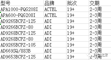
ACTEL, AD part advantageous ordering (full series):
XILINX, ALTERA advantageous stock or ordering (full series):
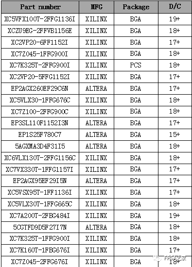
(The above devices are part of the models, for more models please consult group owner Jin Juan)
Service philosophy: FPGA Home Component City aims to facilitate engineers to quickly and conveniently purchase components. After years of dedicated service, our customer service is spread across large listed companies, military research units, and small and medium enterprises. Our greatest advantage is emphasizing the service-first philosophy, and achieving fast delivery and favorable prices!
Directly operated brands: Xilinx ALTERA ADI TI NXP ST E2V, Micron, and more than a hundred component brands, especially skilled in components subject to US sanctions against China.We welcome engineer friends to recommend us to purchasing or consult us personally!We will continue to provide the best service in the industry!

Official thanks to brands in the FPGA technical group: Xilinx, Intel (Altera), Microsemi (Actel), Lattice, Vantis, Quicklogic, Lucent, etc.