EETOP focuses on chips and microelectronics, click on the blue text above to follow us.
 EETOP
EETOP
EETOP Chuangxin Network (Yite Chuangxin): A well-known domestic veteran electronic engineer community and semiconductor industry portal website (1.5 million members)
www.eetop.cn bbs.eetop.cn
blog.eetop.cn edu.eetop.cn
EETOP compiled from allaboutcircuits.In the past month, the FPGA market has been thriving. In this article, we will briefly examine the three latest FPGAs released by Xilinx, Intel, and Lattice.
Each of these FPGAs focuses on different aspects of performance improvement: the Xilinx VU57P attempts to overcome memory bandwidth challenges in demanding applications. The Intel Stratix 10 NX FPGA integrates AI-optimized DSP modules to achieve large AI models with low latency. Additionally, the Lattice Nexus FPGA aims to redefine low power and small size in FPGAs.
Xilinx VU57P FPGA — High Bandwidth Memory
Over the past decade, computational bandwidth in many application areas has grown exponentially. For example, the number of DSP slices provided by Xilinx FPGAs for machine learning applications has increased from about 2,000 slices in the largest Virtex 6 FPGA to about 12,000 slices in modern Virtex UltraScale+ devices.
As shown, a similar trend has been observed in other application areas such as networking and video applications.
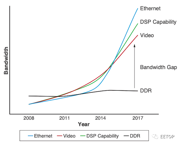
Memory bandwidth requirements
The above figure shows that over the past decade, memory bandwidth for DDR technology has only slightly increased—from DDR3 to DDR4, it has roughly doubled. (Notably, the leap from DDR4 to DDR5 may be even more impactful.)
The bandwidth gap in the figure indicates that the limited data transfer rate between the FPGA and memory is a bottleneck in these applications. To address this issue, designers often use multiple DDR chips in parallel to increase memory bandwidth (not necessarily memory capacity). However, due to high power consumption, size, cost issues, and PCB design challenges, this approach becomes infeasible when memory bandwidth exceeds about 85GB/s.
Furthermore, an effective solution to the memory bandwidth issue is a type of memory based on DRAM known as High Bandwidth Memory (HBM). In this case, silicon stacking technology can be used to implement DRAM memory and FPGA in the same package, as shown in the figure below.
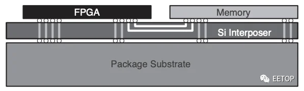
Silicon stacking helps to parallelize DRAM memory and FPGA
HBM technology allows us to eliminate the relatively long PCB traces required to connect DDR chips to FPGAs. Using integrated HBM interfaces with a large number of pins can significantly increase memory bandwidth, with latencies similar to DDR-based technologies.
Xilinx recently released the VU57P FPGA (from the Virtex UltraScale+ series), which integrates 16GB HBM and up to 460GB/s of memory bandwidth. This device features an integrated AXI port switch that allows us to access any HBM memory location from any memory port.
In addition to the energy-efficient computing capabilities and large memory bandwidth discussed above, the VU57P also offers high-speed interfaces such as 100G Ethernet with RS-FEC, 150G Interlaken, and PCIe Gen4. The new device’s 58G PAM4 transceivers support connections with the latest optical standards. This is useful in various applications such as next-generation firewalls and switches and routers with QoS.
Intel Stratix 10 NX FPGA — AI Optimized DSP Modules
Many conventional applications of Digital Signal Processing (DSP) require high-precision arithmetic. This is why FPGAs typically have DSP modules with high-precision multipliers and adders. For example, XC7A50T (Xilinx) and 5CGXC4 (Intel) have 120 and 140 18×18 multipliers, respectively.
It has been shown that many deep learning applications can be implemented with fewer bits without significantly sacrificing accuracy. Lower precision approximations reduce the number of computational resources and the required memory bandwidth.
Another advantage of reducing bit width is that lower precision computations and fewer bits need to be transferred per memory transaction can save power consumption. In fact, according to researchers at UC Davis, in many deep learning applications, INT8 or even lower precision calculations can yield acceptable results.
The Intel Stratix 10 NX FPGA is Intel’s first AI-optimized FPGA. These devices integrate arithmetic blocks known as AI Tensor Blocks, which contain dense arrays of low-precision multipliers. The base precision of these blocks is INT8 and INT4, although they support hardware for FP16 and FP12 numerical formats through shared exponents.
Compared to the DSP modules of the standard Intel Stratix 10 FPGA, the AI Tensor modules (used in Stratix 10 NX FPGA) can increase INT8 throughput by 15 times. The high-level block diagram of the AI Tensor Block is shown below.
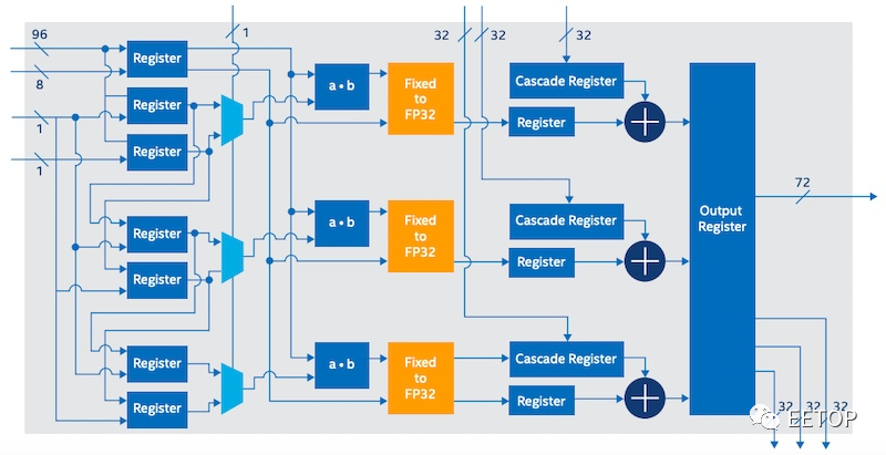
Block diagram of AI Tensor Block
The most notable feature of the Intel Stratix 10 NX FPGA is the high computational density provided by the AI-optimized computing blocks. However, the new device also integrates two additional features that further help designers achieve their large AI models with low latency: it supports rich approximate computing memory (integrated HBM) and high bandwidth networking (up to 57.8 G PAM4 transceivers).
Lattice Nexus — Low Power, Small Size FPGA
Lattice Semiconductor recently released its Certus-NX FPGA series, which uses 28nm fully depleted silicon-on-insulator (FD-SOI) process technology. FD-SOI was initially developed by Samsung and is somewhat similar to traditional CMOS processes. However, as shown in the figure below, it allows for programmable bias for most transistors.
Lattice Semiconductor recently released its Certus-NX FPGA series, which uses 28nm fully depleted silicon-on-insulator (FD-SOI) process technology. FD-SOI was initially developed by Samsung and is somewhat similar to traditional CMOS processes; however, it allows for programmable bias for most transistors, conceptually illustrated below.
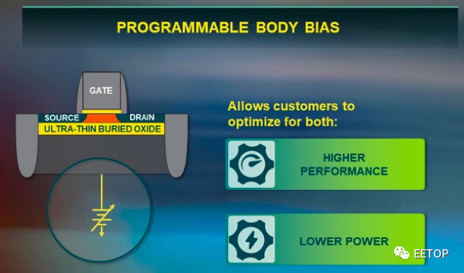
Circuit architecture of the Lattice Nexus platform
Programmable buck voltage significantly reduces chip area and power consumption. Compared to other FPGAs with a similar number of logic units, the power consumption of Certus-NX is reduced by up to four times.
Due to the use of FD-SOI technology, the new device can be as small as 6mm x 6mm, providing up to twice the I/O per mm² compared to similar FPGAs. The table below compares Certus-NX-40 with similar products from Intel and Xilinx.
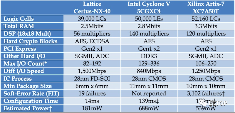
Comparison of Three Popular FPGAs for PCIe Design
It is worth noting that the new device supports AES for bulk encryption and Elliptic Curve (ECDSA) for authentication. Therefore, it can provide higher security for connected devices. Additionally, it has a high tolerance for soft errors, making it suitable for aerospace applications.
FPGA Development Trends
By studying these latest released FPGAs from Xilinx, Intel, and Lattice Semiconductors, we can gain a clearer understanding of how FPGAs are evolving—focusing on higher memory bandwidth, AI optimization, low power consumption, and small size.
Recommended Materials
-
P.E. Allen’s classic lecture on PLL
-
The most comprehensive online semiconductor materials available for free download!
-
The most comprehensive collection of ISSCC 2008~2020 papers + PPT downloads available online
-
Classic semiconductor manufacturing process PPT (2000 pages)
-
Automotive electronics EMC design testing basics (very detailed PPT)
- Super classic materials: Analog Integrated Circuits lecture notes (1008 pages PPT)
 1000 articles! Free premium articles on chip design/manufacturing!
Click to read the original text to enter the EETOP WeChat backend, enter “chip” to get!