
Table of Contents
-
0. Reprint Instructions
-
1. IO Interface Introduction
-
2. IO Logic Resource Introduction
-
3. Advanced IO Logic Resource Introduction
-
4. IO_FIFO Introduction
0. Reprint Instructions
FPGAs are suitable for concurrent data processing, but where does the data come from? This is what this article will discuss.SelectIO — The Vanguard of Data Transmission
There are significant differences between the SelectIO structure of the Ultrascale+ series and the 7 series FPGAs, which will be summarized later.
Original Link:
Xilinx 7 Series FPGA SelectIO Part 1: IO Interface Introduction
https://blog.csdn.net/XiaoQingCaiGeGe/article/details/85255296
Xilinx 7 Series FPGA SelectIO Part 2: IO Logic Resource Introduction
https://blog.csdn.net/XiaoQingCaiGeGe/article/details/85255337
Xilinx 7 Series FPGA SelectIO Part 3: Advanced IO Logic Resource Introduction
https://blog.csdn.net/XiaoQingCaiGeGe/article/details/85255386
Xilinx 7 Series FPGA IO_FIFO Introduction
https://blog.csdn.net/XiaoQingCaiGeGe/article/details/85255414
All original images referenced from
7 Series FPGAs SelectIO Resources User Guide
https://www.xilinx.com/support/documentation/user_guides/ug471_7Series_SelectIO.pdf
1. IO Interface Introduction
Starting from this part, we will discuss the SelectIO of the Xilinx 7 series FPGAs in three articles. SelectIO refers to the general term for I/O interfaces and I/O logic. The SelectIO section can be divided into three parts: the first part introduces the electrical characteristics of I/O, the second part introduces I/O logic resources, and the third part introduces advanced I/O logic resources (serializer/deserializer). In this article, we will talk about the electrical characteristics of I/O in Xilinx 7 series FPGAs.
When discussing I/O, we must first mention the FPGA BANK. In the 7 series FPGAs, BANKs are divided into HR (High-range) BANK and HP (High-performance) BANK. HP BANK only supports I/O signals with voltage levels less than or equal to 1.8V, while HR BANK supports I/O signals with voltage levels less than or equal to 3.3V. HP BANK is designed specifically for high-speed I/O signals and supports DCI (Digitally Controlled Impedance), while HR BANK is suitable for more general I/O signal designs. The following table lists the characteristics of HP BANK and HR BANK.
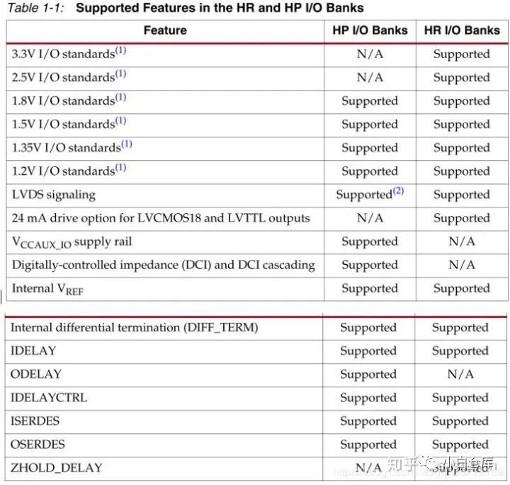
Whether HR or HP BANK, each BANK contains 50 I/O pins, and each I/O pin can be configured as input or output. The first and last pins of each BANK can only be used as single-ended I/O, while the remaining 48 I/O pins can be configured as 24 pairs of differential I/O.
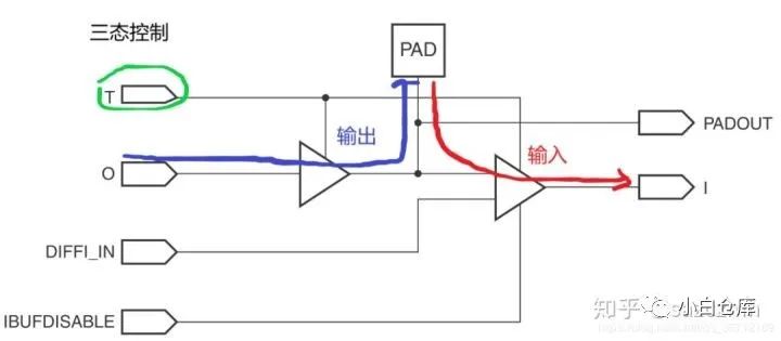
Single-ended I/O pins support common voltage standards such as LVTTL, LVCMOS, HSTL, PCI, etc. Differential I/O pins support LVDS, differential HSTL, and other differential signals. However, the official documentation surprisingly does not describe support for the very common LVPECL differential signal, which is quite strange. The following figure shows a schematic of an I/O interface (IOB):
In summary, the biggest difference in the 7 series FPGAs compared to previous generations is:
-
There is an HP BANK dedicated to high-speed interface signals, which can only support a maximum of 1.8V level.
-
Each BANK has up to 50 I/O.
Other electrical performances remain basically unchanged and do not impact our usage.
2. IO Logic Resource Introduction
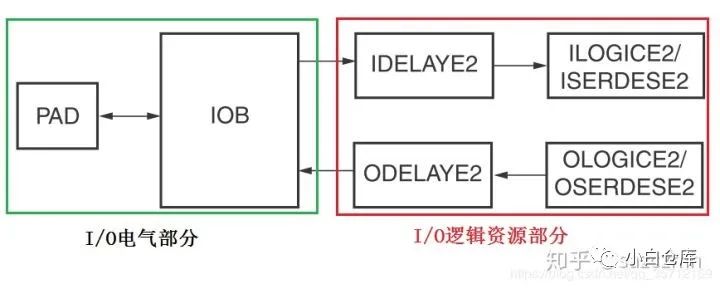
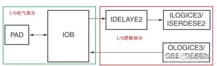
In the previous article, we briefly discussed the electrical characteristics of I/O. In this article, we will continue to introduce I/O logic resources and first present two images. Figure 1 shows the I/O module of HP BANK, and Figure 2 shows the I/O module of HR BANK. The difference is that the latter does not have the ODELAYE module.
The I/O logic resources mainly consist of five parts:
1. ILOGIC
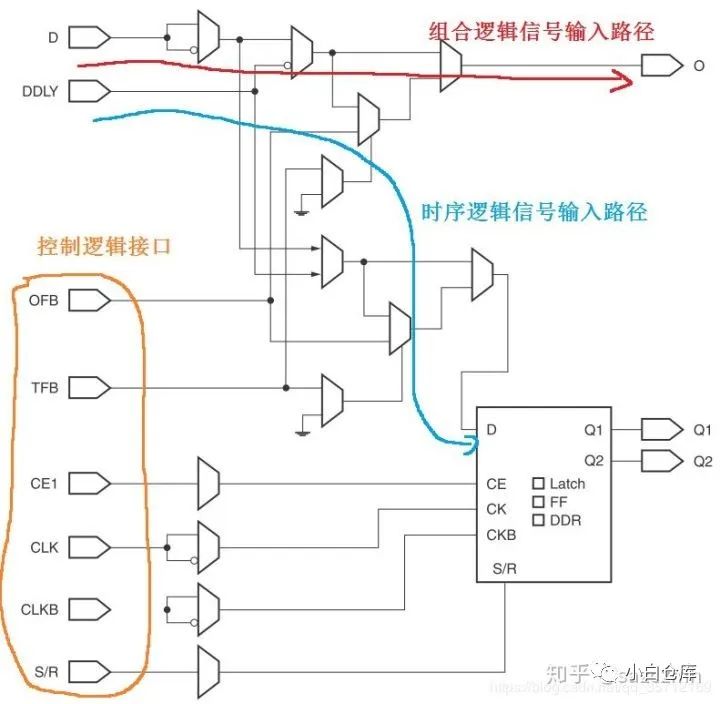
ILOGIC refers to input signal processing logic, which is adjacent to IOB. The external input signal first passes through ILOGIC. ILOGIC is composed of many data selectors and an IDDR (input Double Data Rate) flip-flop. This flip-flop can capture input data on both edges and can also be split into ordinary single-edge flip-flops. In HP BANK, ILOGIC is referred to as ILOGICE2, while in HR BANK, it is referred to as ILOGICE3. The following figure shows a schematic of ILOGICE3:
2. IDELAY
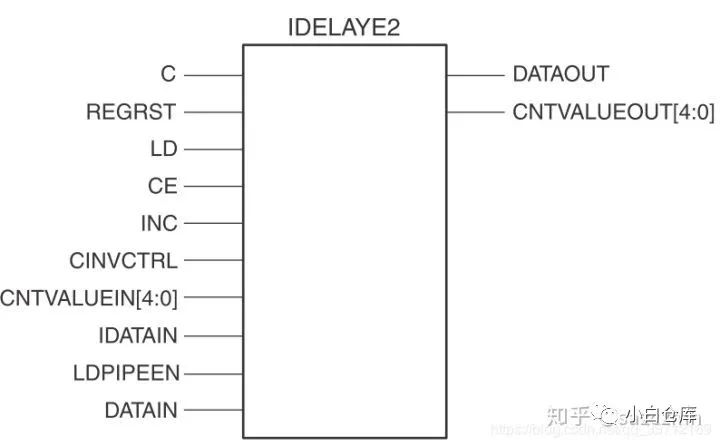
IDELAY is known as the signal delay module, and its function is to delay the signal for a period of time. This is crucial for input signals that need to be aligned. In the 7 series FPGAs, it is referred to as IDELAYE2. IDELAYE2 can delay signals from 0 to 31 segments, adjustable within this range, with a delay precision of approximately 78ps (1/(32×2×FREF), where FREF is the reference clock of IDELAYCTRL). The following figure shows the instantiation block diagram of IDELAYE2.
3. IDELAYCTRL
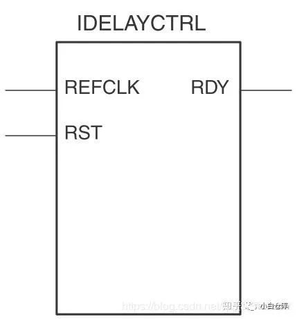
IDELAYCTRL is actually an auxiliary module. To put it simply, as long as we use IDELAY or ODELAY, IDELAYCTRL must be used; otherwise, it cannot function correctly. This is because the delay precision of IDELAY or ODELAY is determined by the input clock of IDELAYCTRL, which is generally 200MHz. The following figure shows the instantiation block diagram of IDELAYCTRL.
4. ODELAY
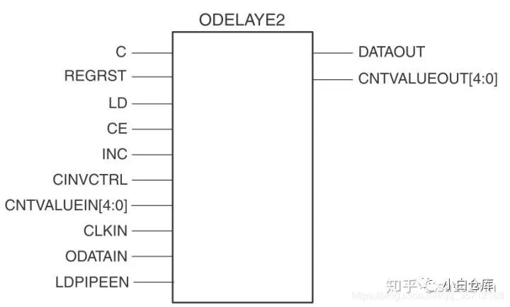
ODELAY works similarly to IDELAY, but it is used for delaying output signals. Additionally, there is no ODELAY in HR BANK; it is only found in HP BANK and is referred to as ODELAYE2. When using ODELAYE2, it is also necessary to instantiate IDELAYCTRL. The following figure shows the instantiation block diagram of ODELAYE2:
5. OLOGIC
OLOGIC consists of two parts: one for configuring the output path and the other for configuring the tri-state control path. Both the output path and tri-state control path can be independently configured as edge-triggered flip-flops, ODDS, and combinational logic outputs.
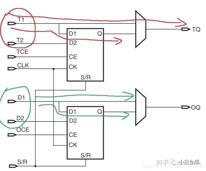
In general, I/O logic resources are used to acquire or output signals. For general low-speed signals, I/O logic resources do not demonstrate their advantages; whether used or not does not affect the final result. However, for high-speed signals, I/O logic resources must be used correctly; otherwise, the entire FPGA logic code will be useless. But isn’t FPGA used to process high-speed signals? Therefore, the I/O section should be the essence of the entire FPGA, and of course, it is also the most challenging part to use…
To facilitate the use of I/O logic resources, Xilinx has specifically grouped several modules introduced in this article to form the powerful ISERDESE2 and OSERDESE2 primitives. By simply calling the primitives and using them correctly, we can complete advanced I/O logic designs. In the next article, we will discuss the advanced logic resources ISERDESE2 and OSERDESE2!
3. Advanced IO Logic Resource Introduction
In the previous article, we introduced IO logic resources. In this article, we will discuss advanced IO logic resources, specifically the ISERDESE2 and OSERDESE2 modules.
The ISERDESE2 module is known as Input serial-to-parallel converters. Its function is to achieve high-speed source-synchronous input data serialization and deserialization.
The OSERDESE2 module is known as output parallel-to-serial converters. Its function is to achieve high-speed source-synchronous output data serialization and deserialization.
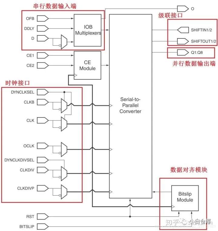
Let’s talk about ISERDESE2 first. This module receives high-speed source-synchronous serial signals from external inputs to the FPGA and converts them into parallel data signals as needed by the user within the FPGA. Figure 1 shows the functional block diagram of ISERDESE2, which can be divided into five functional parts:
1. External Serial Data Input Terminal
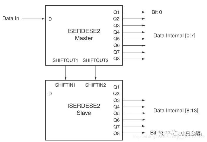
This part receives high-speed source-synchronous data from external inputs, which can be SDR or DDR. In SDR mode, the data conversion width can be 2, 3, 4, 5, 6, 7, or 8 bits. In DDR mode, the data conversion width is 4, 6, or 8 bits. If two ISERDESE2 modules are cascaded, the DDR mode can support 10 or 14 bits.
2. Clock Interface
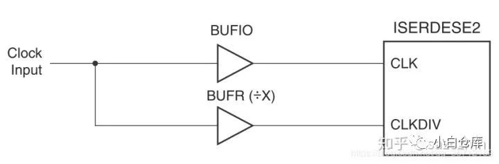
This part provides the high-speed source-synchronous serial clock for ISERDESE2, the clock for acquiring parallel data, and the control clock. Figure 2 shows how to connect the source-synchronous clock to ISERDESE2.
3. Parallel Data Output Terminal
This interface is self-explanatory; it is the parallel data we need. In SDR mode, it is 2, 3, 4, 5, 6, 7, or 8 bits, and in DDR mode, it is 4, 6, 8, 10, or 14 bits.
4. Cascade Interface
This interface is the key to achieving 10 or 14 bits in DDR mode. By cascading with another ISERDESE2, both can complete the serialization and deserialization of 10 or 14 bits of data. Figure 3 shows the usage of two ISERDESE2 modules in cascade.
5. Data Alignment Module
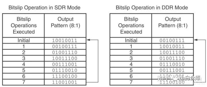
This module is also known as the Bitslip module, used to align the boundaries of parallel data. For example, if we have 8 bits of serial data from external input, after serialization and deserialization, we can obtain 8 bits of parallel data, but this parallel data may be misaligned between the front and back 8 bits of data, which serialization and deserialization cannot identify. Therefore, Bitslip is specifically used to find the boundary of the desired parallel data.
Figure 4 shows how Bitslip determines the boundary of parallel data: for SDR mode, enabling Bitslip once shifts the data left by one position; for 8-bit parallel data, moving 8 times completes a cycle, and this can continue infinitely until the user-defined parallel data is found. For DDR mode, Bitslip works differently; enabling Bitslip once shifts the data right by one position or left by three positions, alternating between the two, completing a cycle in 8 moves.
Now let’s talk about the OSERDESE2 module. This module differs from the ISERDESE2 module in that it lacks the Bitslip module but includes a tri-state control module, which can implement tri-state control for serialization and deserialization. The data width rules are the same as those for the ISERDESE2 module. Figure 5 shows its functional block diagram:
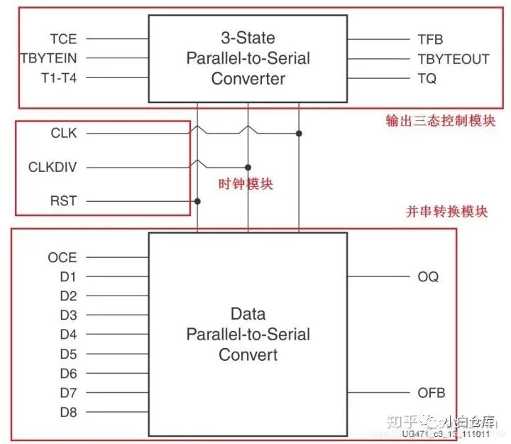
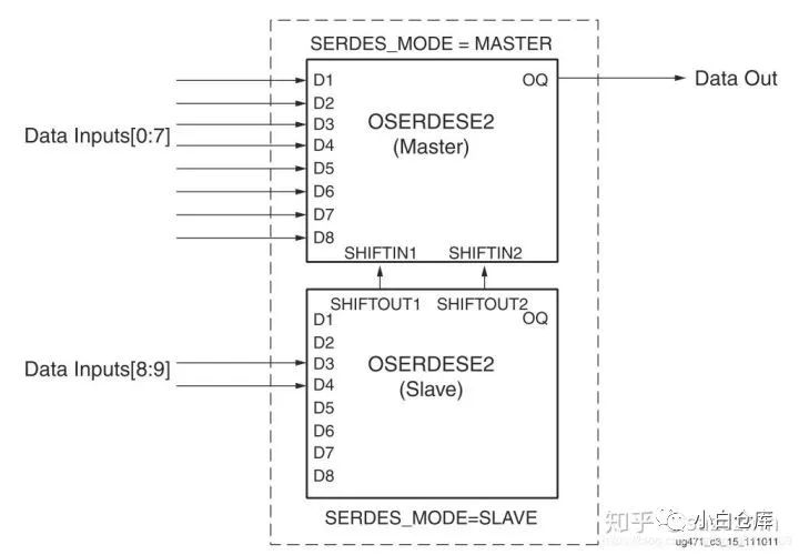
Figure 6 shows the cascade design of OSERDESE2, achieving 10 and 14 bits of serialization and deserialization:
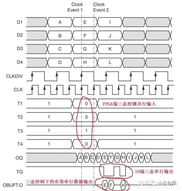
Besides the additional tri-state control module, OSERDESE2 is basically the same as ISERDESE2, only with inverted data flow operations. Therefore, we mainly focus on the tri-state control module, which primarily functions to implement tri-state output of serial data flow. Figure 7 provides the detailed timing structure of tri-state control. From the figure, we can see that under tri-state control, the serial data flow has selective outputs E, F, and H, achieving tri-state control of the output serial data.
This article briefly introduced ISERDESE2 and OSERDESE2. Do you understand? Of course, if you want to use them practically, we still need to look at the specific data manuals! As mentioned in the previous article, the I/O part is the most complex part of the FPGA and the most challenging to design. To become familiar with its use, we need to work hard and study!
4. IO_FIFO Introduction
In the first three articles, we introduced SelectIO logic resources. In this article, we will discuss another concept that is closely integrated with SelectIO logic resources and complements each other — IO_FIFO.
One IO_FIFO includes one IN_FIFO and one OUT_FIFO. It is a new design of IO-specific FIFO in the 7 series FPGA, mainly used for extending the logic functions of IOLOGIC (such as ISERDES, IDDR, OSERDES, or ODDR).
Each BANK of the FPGA has 4 IN_FIFO and 4 OUT_FIFO, which means that every 12 I/Os correspond to one IN_FIFO and one OUT_FIFO.
IN_FIFO receives 4-bit wide input data from ILOGIC but can output 4-bit or 8-bit wide data to the FPGA internal SLICE. OUT_FIFO does the opposite, receiving 4-bit or 8-bit wide input data from OLOGIC but outputting 4-bit wide data.
Each IO_FIFO has a storage size of 768 bits and can be configured as 12 groups of 4×4-bit wide data FIFO or 10 groups of 4×8-bit wide data FIFO. The depth of each IO_FIFO is 9. Figure 1 shows the structural diagram of IO_FIFO:
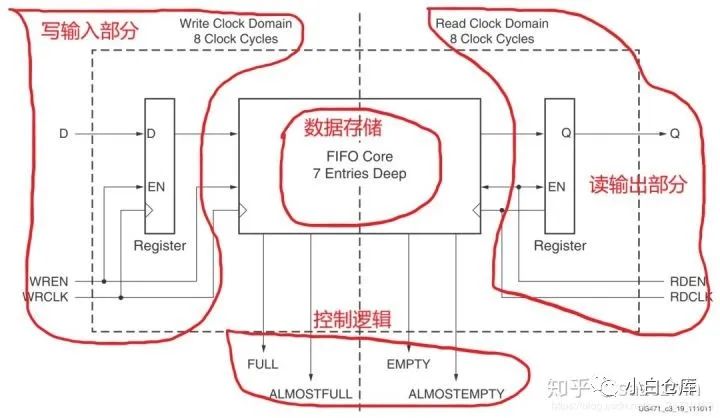
Figure 2 shows the primitive block diagram of IN_FIFO:
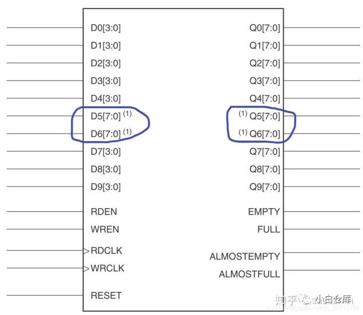
As mentioned earlier, when configured as 12 groups of 4-bit wide input and 4-bit wide output, input D0[3:0]~ D9[3:0] corresponds to output Q0[3:0]~ Q9[3:0]; input D10[3:0] corresponds to input D5[7:4], and output Q5[7:4]; input D11[3:0] corresponds to input D6[7:4], and output Q6[7:4].
When configured as 10 groups of 4-bit wide input and 8-bit wide output, D0[3:0] ~ D9[3:0] corresponds to output Q0[7:0]~ Q9[7:0]; at this time, the write clock frequency is twice that of the read clock frequency. The operation process of OUT_FIFO and IN_FIFO is exactly the opposite, so we will not elaborate here.
In summary, IO_FIFO is essentially a regular FIFO with a smaller storage depth and a fixed width of 4/8 bits. The 7 series FPGA has specifically designed such a FIFO, which is more suitable for byte/half-byte data buffering at the I/O interface.
Source: https://blog.csdn.net/weiaipan1314/article/details/110198593?utm_medium=distribute.pc_relevant.none-task-blog-2~default~baidujs_utm_term~default-0.pc_relevant_default&spm=1001.2101.3001.4242.1&utm_relevant_index=3
Copyright belongs to the author