Xilinx FPGA Hardware Design (Part 3): Power Supply Design

Xilinx FPGA Hardware Design (Part 3): Power Supply Design

Power supply design is also a very important aspect of FPGA design. The following explains the power supply design for the 7 series FPGA. 1.Introduction to FPGA Power Supply Types The LVCMOS standards supported by the 7 series FPGA are: LVCMOS12, LVCOMS15, LVCMOS18, LVCMOS25, and LVCMOS33. Among them, LVCMOS25 and LVCMOS33 I/O standards can only … Read more
Analysis of the Header Information in Xilinx FPGA Bitstream Files

Analysis of the Header Information in Xilinx FPGA Bitstream Files

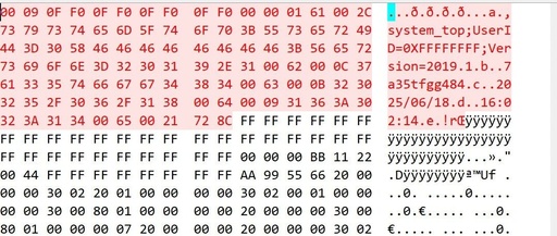
Xilinx FPGA configuration files, in .bit and .bin formats, are binary configuration data files. The .bit file includes header information that is not required to be programmed into the FPGA. In some loading or remote update scenarios, both types of configuration files can be used, but using the .bit file provides additional information. The length … Read more

Xilinx Chip Inventory

Xilinx Chip Inventory

XCZU48DR-2FFVG1517IXCZU47DR-2FFVG1517IXC7A100T-2FGG484C XC95144XL-10TQG144C XC95144XL-10TQG100CXC6SLX16-2FTG256CXC6SLX9-2FTG256CXC3S500E-4PQG208IXC7A50T-2FGG484CXC3S200AN-4FTG256IXC6SLX9-2CSG324IXC3S400A-4FTG256CXC6SLX100T-2FGG484CXC6SLX9-2CSG324CXC6SLX9-2FTG256C XC6SLX25-3FTG256CXC6SLX25-2CSG324IXC6SLX75T-3FGG484CXC6SLX45-2FGG484CXC3S250E-4PQG208IXCZU2CG-1SFVC784EXCZU7EV-2FBVB900E XCZU67DR-2FFVE1156IXCZU19EG-2FFVD1760IXC95108-15PQ100CXC9536-15PC44CXC18V02PC44CXC18V04VQ44CXC7272A-25PC84CXC7A75T-1FGG676I XC9536XL-10VQ64CXC3S400AN-4FGG400CXCZU2CG-1SBVA484EXC3S250E-4VQG100IXC7A15T-1CSG324CXC6SLX100-2FGG676IXC6SLX25-2CSG324CXC7K325T-2FFG900IXC9572XL-10VQG44CXC5VLX110-1FFG1153CXCKU060-1FFVA1156CXC3S400AN-4FGG400CXC6SLX150-2CSG484IXCZU4EV-2FBVB900EXC3S400AN-4FGG400C XC6SLX16-2CSG225CXC7Z020-1CLG484CXC7VX690T-2FFG1926IXC7A200T-2FBG676IXCVU095-2FFVC2104E XC7K325T-2FFG676CXC7K70T-1FBG484IXC7A50T-2FGG484C XC7A200T-2FBG676IXC3S400A-4FTG256IXC3S400AN-4FTG256IXC95288XL-10TQG144IXCZU19EG-2FFVC1760IXCKU095-1FFVA1156IXCVU190-2FLGB2104IXCVU190-2FLGB2104IXC18VO4Q44IXCKU15P-2FFVA1156EXC7A50T-2FTG256CXCZU11EG-2FFVC1760IXC7A35T-1CSG325C XCF04SVOG20CXCKU040-2FFVA1156EXCZU47DR-2FFVA1156IXCZU21DR-2FFVD1156IXC7A50T-1FGG484CXC7Z010-2CLG400IXC7K160T-2FFG676IXCKU060-1FFVA1156IXCKU060-2FFVA1156IXC7K410T-2FFG900IXC3S1400A-5FGG484CXC7Z030-1FBG484CXC7A75T-2FGG676CXC6SLX100-2FGG484I XC6SLX100-3FGG484CXC6SLX75-3FGG484I XC7Z035-2FBG676EXC6SLX16-2FTG256IXCV50-5FG256IXC7K410T-2FFG676IXC7VX690T-2FFG1761IXCKU035-2FFVA1156IXC7Z030-2FBG484IXC6SLX16-2CSG324C

Differences Between Various Levels of Xilinx FPGAs

Differences Between Various Levels of Xilinx FPGAs

Xilinx FPGAs have the following main differences across commercial, industrial, automotive, defense, and aerospace grades: 1. Operating Temperature Range Commercial Grade: Generally from 0℃ to +70℃, suitable for ordinary commercial electronic devices in indoor normal temperature environments, such as computers, mobile phones, and other consumer electronics. Industrial Grade: Typically from –40℃ to +85℃, capable of … Read more

Comparison of FPGA and Programmable SoC Chips: Analysis of Core Products from Three Major Manufacturers

Comparison of FPGA and Programmable SoC Chips: Analysis of Core Products from Three Major Manufacturers

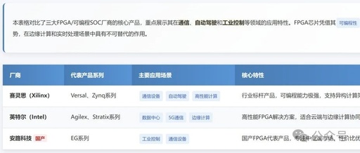
FPGA and programmable SoC chips are important components in modern technology, playing a critical role in various fields such as communication, autonomous driving, and industrial control. Their unique programmability and parallel computing capabilities provide irreplaceable advantages in edge computing and real-time processing scenarios. Below is a detailed analysis of the core products from three major … Read more

FPGA Chip Naming Conventions: A Guide to Decoding Manufacturer ‘Jargon’

The naming of FPGA models is akin to the “identity card” of chips, containing key information such as architecture, process technology, and performance. Mastering these rules allows for quick identification of device characteristics, helping to avoid pitfalls in selection. This article analyzes the naming logic of four major manufacturers (Xilinx, Intel, Lattice, Microchip), enabling you … Read more

Can Xilinx FPGA General IO Be Directly Connected to PLL as Clock Input?

Can Xilinx FPGA General IO Be Directly Connected to PLL as Clock Input?

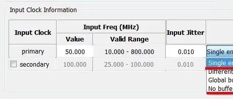
[Conclusion] General IO cannot be directly used as a clock input for PLL; dedicated clock pins can be used instead. General IO can be connected to the PLL clock input through a BUFG, but the PLL settings must be modified to select “No Buffer” for the input clock option. The specific internal layout can be … Read more

The Dual Giants Go Solo: A New Era for FPGA as It Turns Forty

The Dual Giants Go Solo: A New Era for FPGA as It Turns Forty

In 2025, a low-key yet monumental invention in the semiconductor industry—FPGA (Field Programmable Gate Array)—will celebrate its fortieth anniversary. This is not just a milestone in time, but rather a dramatic historical metaphor. In this special year of turning forty, the two giants that once dominated the FPGA market for decades, Xilinx and Altera, after … Read more

Celebrating 40 Years of FPGA Innovation

Celebrating 40 Years of FPGA Innovation

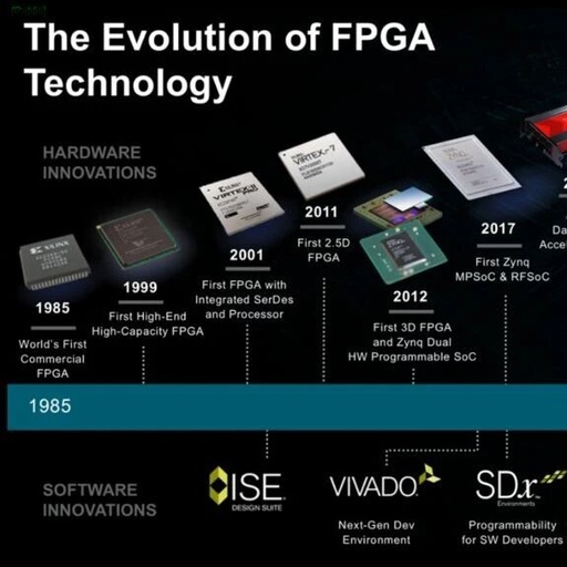
Forty years ago, Xilinx introduced a revolutionary device that allowed engineers to use logic programming right at their desks. The Field Programmable Gate Array (FPGA) developed by Xilinx enabled engineers to download bitstreams with custom logic to desktop programmers for immediate execution, eliminating the weeks of waiting for chips to return from the foundry. If … Read more