Welcome FPGA engineers to join the official WeChat technical group.
Clickthe blue textto follow us – FPGA Home, the best and largest community for pure FPGA engineers in China
ISE version is 14.7
1. Clock IP Core (Clocking Wizard)
Page one
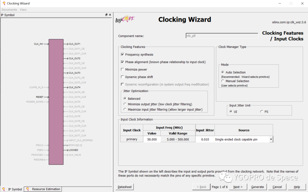
In the Clocking Features options box:
(1) The Frequency synthesis option allows the output clock to have a different frequency than the input clock.
(2) The Phase alignment option refers to phase locking, which means synchronizing the output phase with a reference clock, mostly with the input clock.
(3) The Minimize power option aims to reduce power consumption, which replaces phase and frequency deviations; it can be used when clock requirements are not high and resources are limited, but it is generally not recommended to select this option.
(4) The Dynamic Phase Shift option provides dynamic phase shift functionality; after selecting this option, the phase shift can be controlled at the input side, with feedback after the phase shift is completed, and the phase shift step length is fixed to several values.
In the Jitter Optimization options box:
(1) Balanced means selecting a relatively balanced bandwidth during jitter optimization (generally select this one).
(2) Minimize output jitter: minimizes the jitter of the output clock, but may increase power consumption or resources, possibly leading to output phase errors.
(3) Maximize input jitter filtering: this option allows the input clock jitter to increase but may lead to increased output clock jitter.
Other options are selected as shown in the image.
Page two
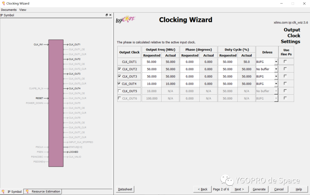 Select output CLK port
Page three
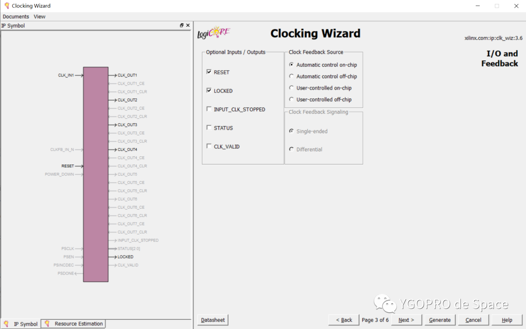
Optional ports can be selected based on actual applications; generally, select reset and locked.
Page four
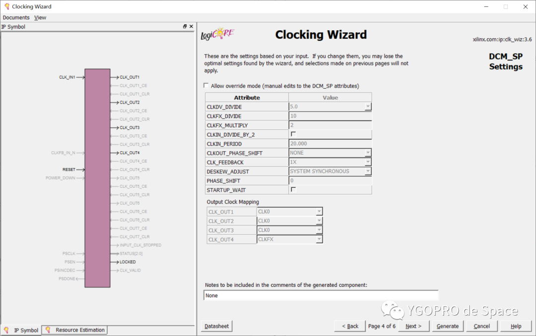
Page five
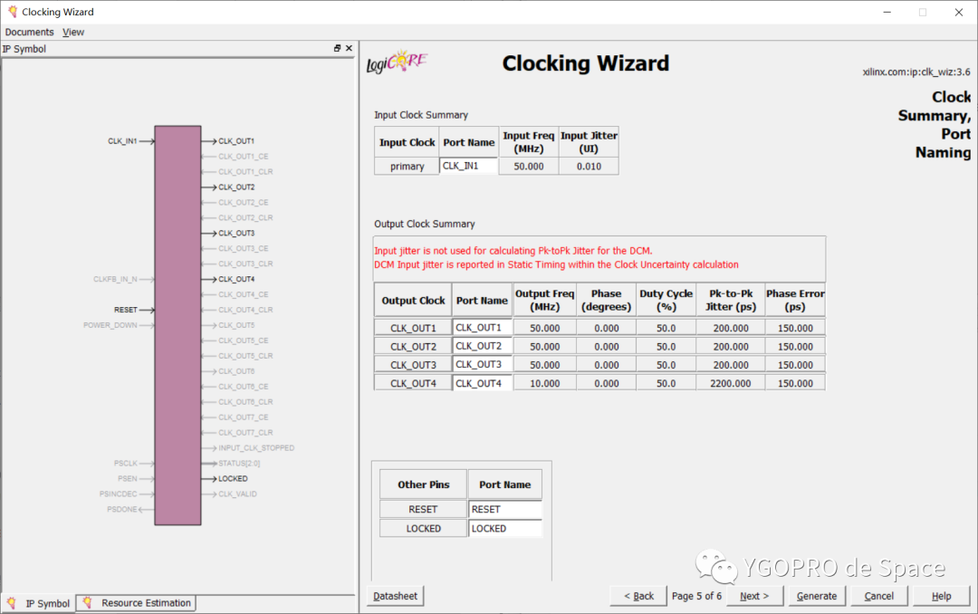
Ports can be renamed.
2. FIFO IP Core (FIFO Generator)
FIFO is a first-in-first-out data storage and buffer, essentially RAM. The width of FIFO is the bit width of each data, and the depth of FIFO simply refers to how many data items need to be stored. FIFO can be synchronous or asynchronous; synchronous means the read and write clocks are the same, while asynchronous FIFO means the read and write clocks are different. Generally, asynchronous FIFO is used more often to handle cross-clock domain issues.
Page one
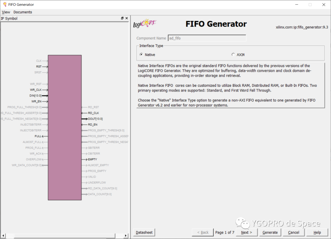
Select Native type for the interface type; AXI4 is used when communicating with DMA or other devices with AXI4 interfaces.
Page two
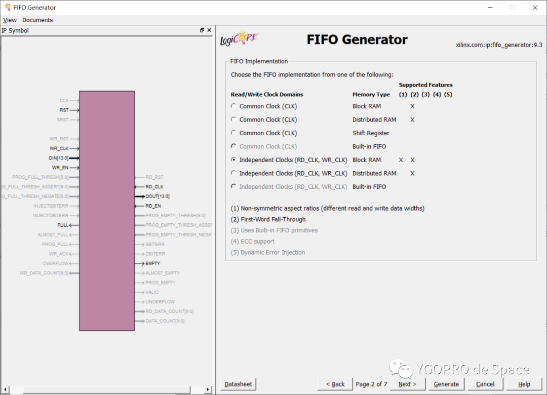
(1) Choose asynchronous clock; the main function of FIFO is to act as a buffer in asynchronous clock domains, so selecting the independent clock mode has a wider range of applications.
(2) Memory Type: The commonly used types are Block RAM and Distribution RAM; the former uses on-chip ROM as a cache, while the latter uses LUT logic resources to build RAM cache. If the FIFO is not large or resources are sufficient, use Block RAM.
Page three
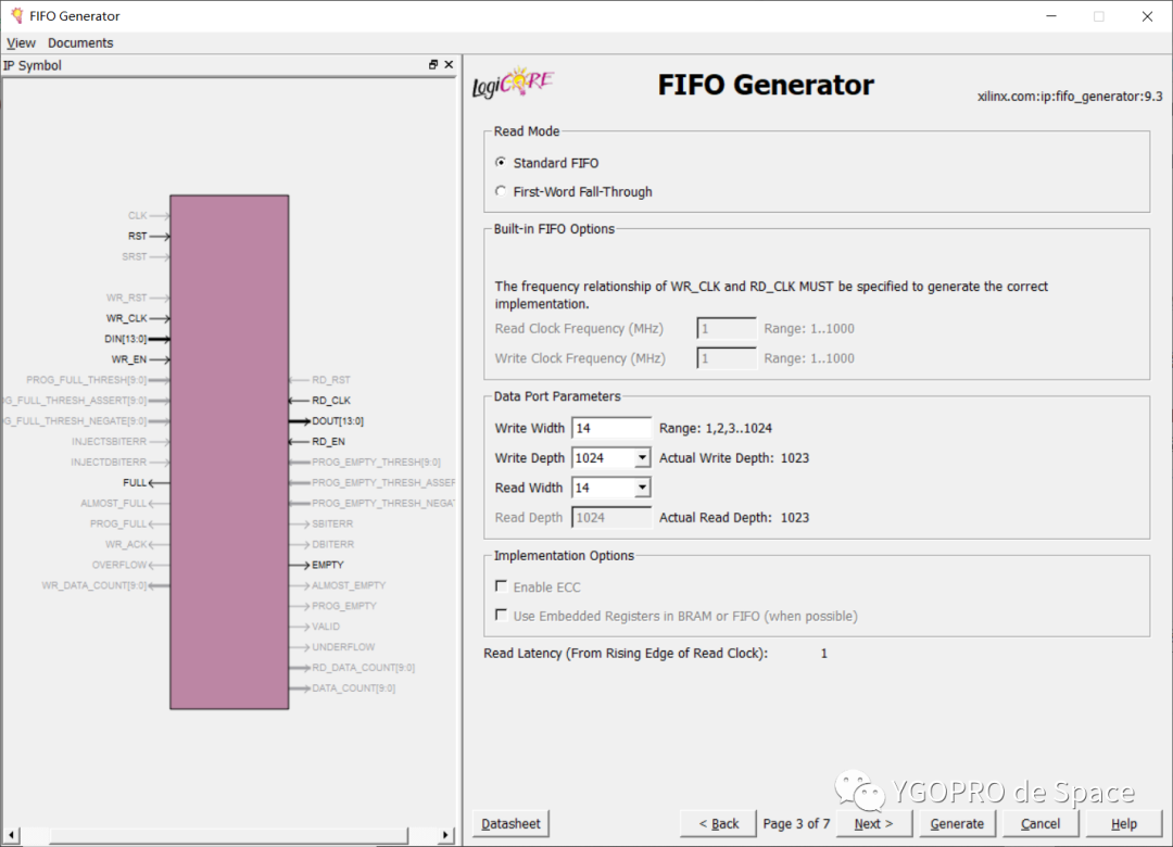
(1) Read Mode: The difference between First-word Fall-Through and Standard FIFO is that Standard FIFO delays data by one clock cycle after enabling read; First-Word Fall-Through immediately provides data upon enabling read.
(2) Set the width and depth according to your needs.
Page four
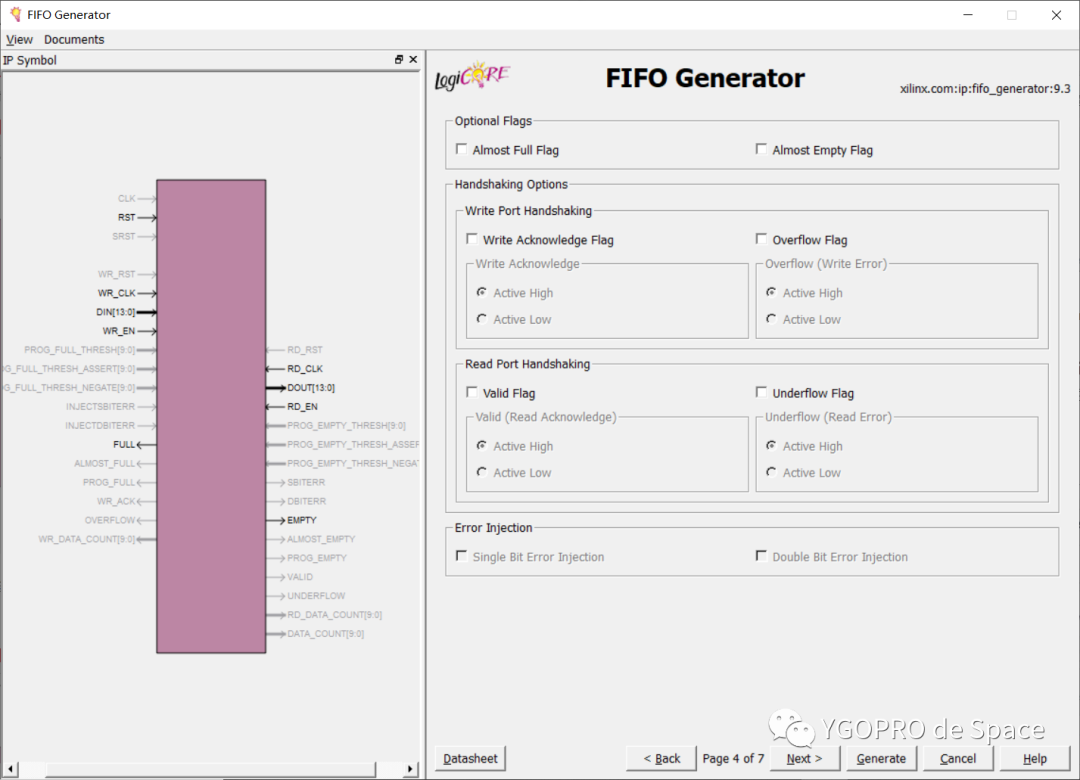
Almost Full Flag and Almost Empty Flag indicate when the FIFO is nearly full/empty; select based on your needs.
Page five
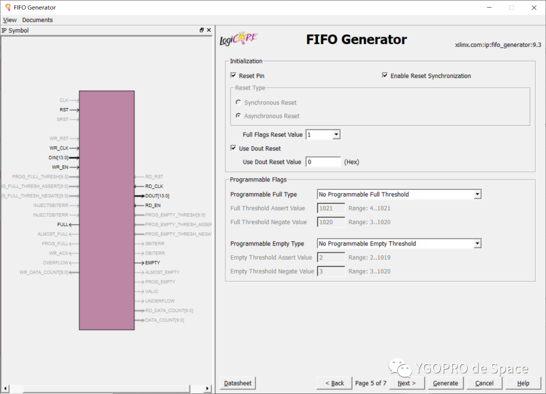
Programmable Full Type and Programmable Empty Type allow you to set how many data items in advance to alert you that it is about to be full or empty.
Page six
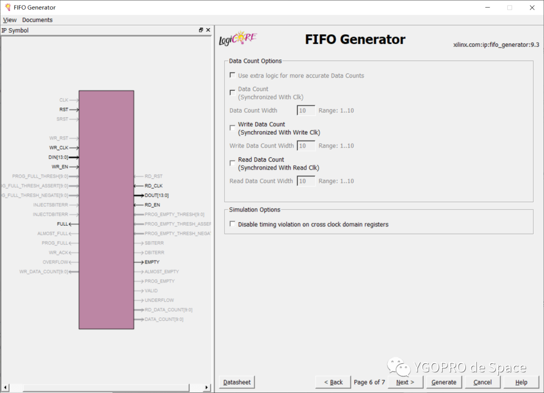
Default settings
Page seven
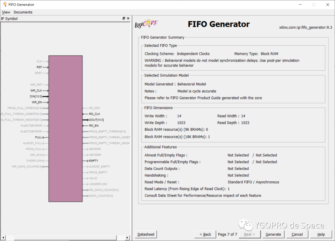
Finally, the report of the configured FIFO is provided; click generate to create the IP core.
3. RAM IP Core (Block Memory Generator)
Page one
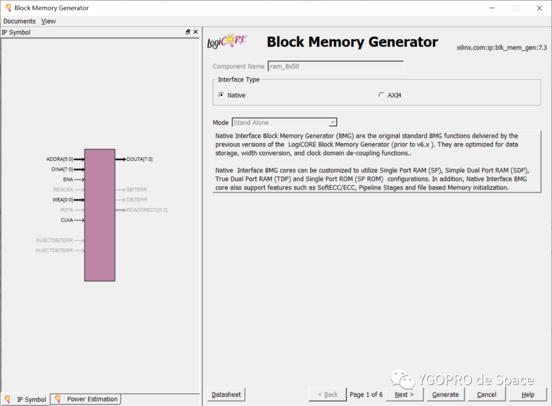
Select Native for Interface Type
Page two
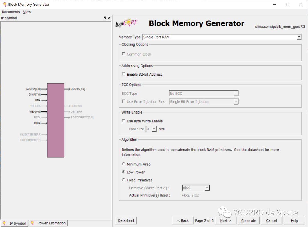
Single Port RAM: Single-port RAM
ADDRA is the address line DINA is the data input ENA is an optional port, enabled only when it is high WEA is write enable; when it is high, DINA data will be written to the corresponding address DOUTA is the A output CLKA is the clock line
Page three
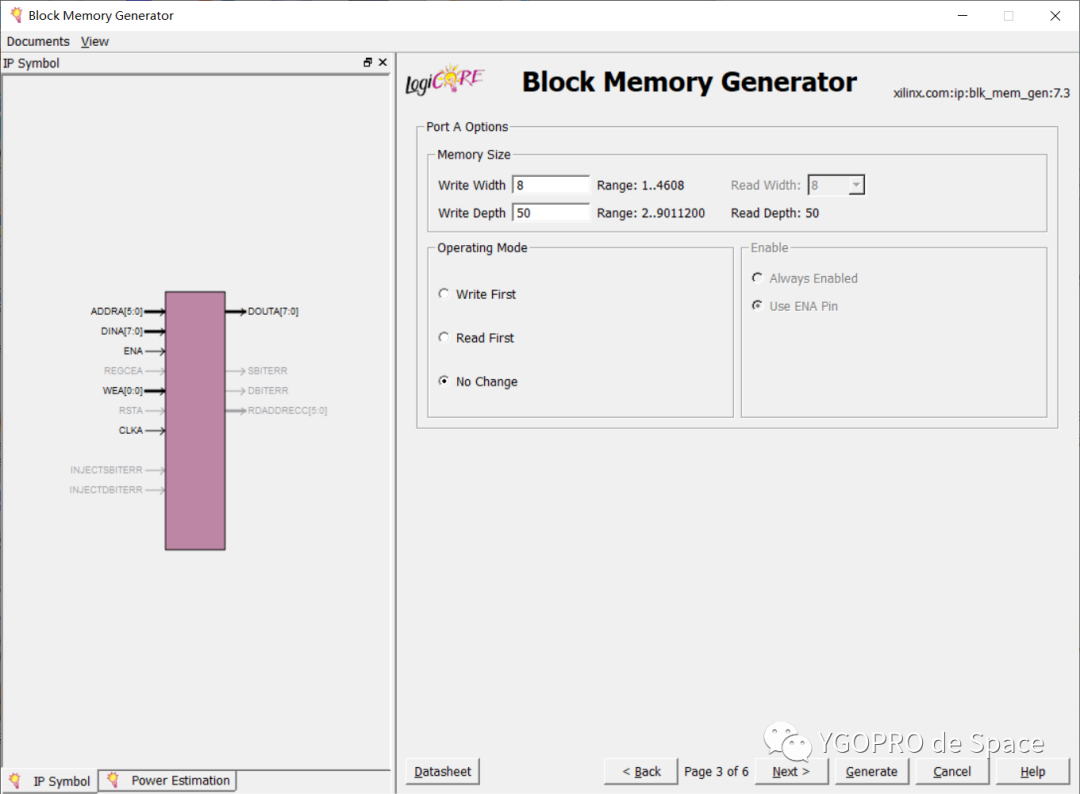
Configure the write width and depth
Page four
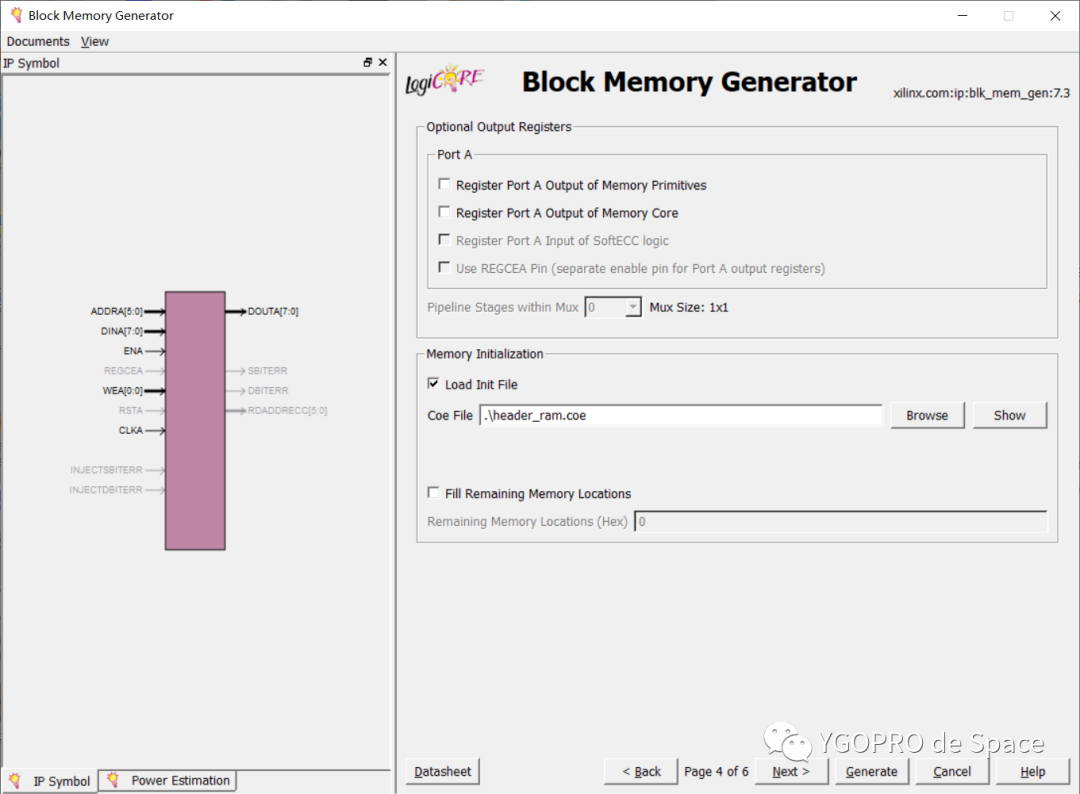
Load coe file:
memory_initialization_radix = 10; // data radix
memory_initialization_vector =1,2,3; // data, ends with a semicolon
Pages five and six
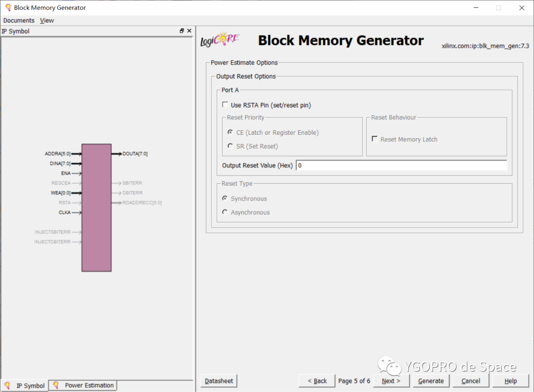
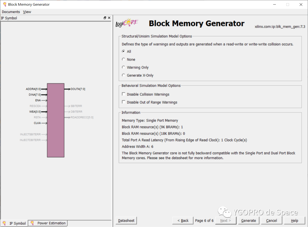
Default settings.

Scanto follow
FPGA Home

Welcome engineers in FPGA, embedded systems, signal processing, etc., to follow our official account.
Follow meengineers!
All the best!
The largest FPGA technical group community in the country

Everyone is welcome to join the largest and strongest FPGA WeChat technical group; this community has tens of thousands of engineers, a group of engineers who love technology, and here FPGA engineers help and share with each other, creating a strong technical atmosphere!Hurry up and invite your friends to join!

Just press and hold to join the national FPGA technical group!

One of the best suppliers of Xilinx and Altera chips in China!
Platform self-operated, imported original quality guaranteed!
Continuously supplying multiple military research institutes and listed companies!
The best FPGA chip prices and the best after-sales service!
With the industry’s top service reputation!
Global top supplier quality standards endorsement!
Full range of XILINX orders or stock advantages!
XCVU9P-2FLGB2104I 200PCS
XCVU9P-2FLGA2104I 500PCS
XCVU13P-2FLGB2104I 300PCS
XC7K325T-2FFG900I 1500PCS
XC7K325T-2FFG676I 950PCS
XC7K160T-2FFG676I 850PCS
XC7VX690T-2FFG1927I Coming soon, please reserve!
XC7VX690T-2FFG1761I Coming soon, please reserve!
For more Xilinx model inquiries, please consult us! Thank you! Scan the QR code to contact us!
Official thanks to FPGA technical group brands: Xilinx, Intel (Altera), Microsemi (Actel), Lattice, Vantis, Quicklogic, Lucent, and others for their support of the technical group!