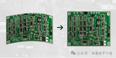
📌 Problem Overview
BGA components are prone to deformation during the reflow soldering process due to high thermal stress. This deformation can lead to poor contact between BGA solder balls and pads, resulting in cold solder joints, short circuits, or solder joint fractures due to stress concentration in later usage. The following table summarizes the core solutions:
| Solution Direction | Specific Measures | Key Points |
|---|---|---|
| Prevent Deformation | Optimize Design and Process | Use high Tg materials, increase board thickness, optimize layout, use fixtures, adjust temperature profiles |
| Measurement Standards | Define warpage acceptance criteria | IPC standard: General SMT board warpage ≤ 0.75%, others ≤ 1.5% |
| Detection Equipment | Identify deformation and stress | Offline detection: Board warpage inspection machine; Online monitoring: Stress-strain tester |
| Remediation After Deformation | Enhance solder joint reliability | Use underfill process, optimize stencil openings and solder paste volume |
🛡️ How to Prevent PCB Deformation
Prevention is key and can be approached from materials, PCB design, and process aspects.
1. Material Selection and PCB Design
Select high Tg materials: Tg (glass transition temperature) is the critical point at which materials transition from a glassy state to a rubbery state.The higher the Tg value, the better the material’s ability to maintain rigidity under high temperatures during reflow soldering, thus enhancing its deformation resistance. However, high Tg materials typically come at a higher cost.
-
Appropriately increase board thickness: Many lightweight electronic products use board thicknesses of 1.0mm or even 0.6mm, which arevery prone to deformation during reflow soldering. If there are no strict thickness limitations, it is recommended to increase the board thickness to1.6mm, which can significantly enhance rigidity and reduce the risk of deformation.
-
Optimize PCB layout and panel design:
-
Reduce board size and minimize panel quantity: The larger the board size, the more severe the sagging and deformation due to its weight on the reflow oven chain. Reducing board size and minimizing panel quantity can help alleviate this issue.
-
Pass through the reflow oven with the long edge vertical to the oven direction: Positioning thelong edge of the PCB as the edge in contact with the reflow oven chain can reduce deformation caused by weight.
-
Avoid shallow V-Cuts: V-Cuts can significantly damage the structural strength between boards, so it is advisable toavoid using V-Cuts or reduce their depth. Usingrouters for panel separation is a better choice.
2. Process Optimization and Auxiliary Tools
-
Adjust the reflow soldering temperature profile: Temperature is the main cause of stress. Byappropriately lowering the peak temperature of reflow soldering orslowing the heating and cooling rates, thermal stress-induced deformation can be reduced. However, it should be noted that excessively slow cooling rates may lead to solder bridging and other issues.
-
Use fixtures: This is a very effective method for dealing with already deformed or high-precision boards.
-
Single-layer fixtures: Can provide support for the PCB, reducing softening deformation above the Tg temperature point.
-
Double-layer fixtures: If single-layer fixtures are ineffective, usingtop and bottom fixtures to clamp the PCB can significantly reduce deformation during passage through the reflow oven, but the fixtures themselves are expensive and require manual placement and retrieval.
📏 PCB Warpage Standards and Detection Methods
1. Warpage Standards
According to IPC standards, there are clear acceptance ranges for PCB warpage:
-
Boards with surface mount devices (SMT): Maximum allowable warpage is 0.75%.
-
Other boards (such as through-hole components): Maximum allowable warpage is 1.5%.
It is worth noting that for some applications with higher requirements, such as BGA packages, customers may request to raise the standard to0.5% or even0.3%.
2. Measurement and Calculation of Warpage
The industry-standard measurement method is as follows:
-
Place the PCB to be measuredflat on a standard calibration platform such as marble or glass.
-
Measure the vertical distance between the highest point of the PCB warpage and the platform, which is the arch height.
-
Calculate using the formula:Warpage = (Arch Height / Length of PCB Long Edge) × 100%
🔬 PCB Deformation and Stress Testing Equipment
To accurately measure PCB deformation and stress, specialized equipment is required.
| Equipment Type | Principle/Features | Application Scenarios | Representative Equipment/Vendor |
|---|---|---|---|
| Board Warpage Inspection Machine | Non-contact, automatic detection | End of production line, offline full inspection of finished boards or copper-clad boards | Zhengtai Technology Board Warpage Inspection Machine |
| Thermal Warpage/Deformation Measuring Instrument | Non-contact, can be paired with temperature control systems | Simulate reflow soldering temperature changes, measure board warpage during thermal processes | Zhizhong Instrument SCW-128 |
| Stress-Strain Testing Instrument | Patch sensors, multi-channel synchronization | Real-time monitoringof SMT, panel separation, assembly testing, etc. throughout the manufacturing process | Yuhua Measurement and Control YST120 Series |
-
Board Warpage Inspection Machine: Suitable for rapid and efficientfull inspection of finished products, ensuring that delivered PCBs meet warpage standards.
-
Thermal Warpage Measuring Instrument: Very suitable for R&D and process optimization stages, used to evaluate the deformation resistance of specific materials or designs under simulated reflow soldering temperatures.
-
Stress-Strain Testing Instrument: This type of equipment canaccurately measure the microscopic strain (με) that the circuit board actually experiences under various processing and testing conditions such as panel separation, insertion, screw tightening, and drop testing by attaching strain gauges to the PCB. This helps identify specific processes that lead to excessive stress and improve them.
🧰 Remedial Measures After PCB Deformation
If the PCB has slight deformation and cannot be changed, the following measures can be taken to ensure the reliability of BGA solder joints:
-
Use Underfill Process:
-
After completing BGA soldering, a special epoxy resin adhesive is allowed to penetrate through capillary action between the BGA chip bottom and solder balls.
-
Once the adhesive cures, it can securely bond the BGA chip, solder balls, and PCB together, forming a unified structure.
-
This cansignificantly enhance the mechanical strength of the solder joints, resisting stress caused by subsequent PCB deformation and effectively preventing solder joint fatigue fractures. This is a key technology commonly used in high-reliability products.
-
Optimize Stencil Design to Adjust Solder Paste Volume:
-
For known areas of PCB deformation, the stencil opening sizes and shapes can be locally adjusted to increase the solder paste printing volume in the recessed areas.
-
Additional solder during reflow can provide a larger solder joint volume, compensating for poor coplanarity caused by board warpage, ensuring that all solder balls can form reliable connections.
💎 Summary and Recommendations
In addressing the PCB deformation issues in BGA reflow soldering, it is recommended to adopt a systematic approach:
-
Prioritize Prevention: Choose high Tg materials and 1.6mm board thickness during the product design phase, and avoid designs that are prone to deformation in layout.
-
Process Optimization: Carefully adjust the reflow soldering temperature profile, and for complex boards, investing in fixtures is a cost-effective solution.
-
Strict Monitoring: Utilize professional detection equipment to monitor warpage of incoming materials and finished boards against IPC standards, and conduct stress testing and control on key manufacturing processes.
-
Post-Processing Reinforcement: For deformed or high-reliability BGA, underfilling is an effective means to enhance long-term reliability.
I hope this information helps you effectively address the challenges of BGA soldering. If you can share more specific product types (such as board size, thickness, etc.), I may be able to provide more targeted advice.