<code class="language-plaintext"><span><span>∆</span></span>
When you think of 3D printing, you might picture plastic figurines or uniquely shaped industrial parts. In fact, this technology has “secretly” evolved to an unexpected level.
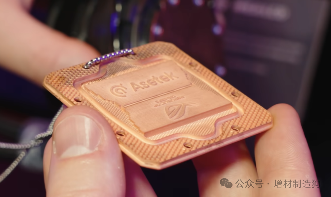
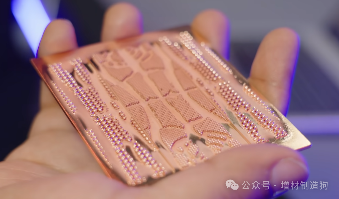
Imagine if 3D printing could not only create a standalone part but could directly penetrate into the core chips of phones and computers, “growing” a pure copper heatsink like a crop? This sounds a bit sci-fi, but this is exactly what is happening, attempting to fundamentally solve the overheating problem that all high-performance electronic products face.
This article will guide you “painlessly” into this novel field called “Additive Electronics.” We will start with a company called Fabric8Labs to see how 3D printing is breaking into the cutting-edge world of semiconductors.
-0- Key Highlights -0-
– Technical Singularity: Decoding Fabric8Labs’ ECAM technology, examining how it directly “prints” heatsinks on chips with three major advantages: “room temperature, pure copper, and integration,” challenging the physical limits beyond Moore’s Law.
– Evolution Path: From Nano Dimension’s “circuit board-level” printing to Fabric8Labs’ “chip-level” precision carving, analyzing the revolutionary evolution of Additive Electronics (AME) from macro to micro, from system to core.
– China’s Position: A deep comparison of domestic and international technology landscapes. Why does China lead in “system-level” cooling applications but face challenges in “chip-level” micro-manufacturing? Where is the breakthrough point for “rooted in the world, developing in China”?
– Business Insights: Analyzing how Additive Electronics reshapes the semiconductor, communication, and data center supply chains. In the global technology ecosystem, where will future investment opportunities and business models head?
-1- Fabric8Labs and ECAM -1-
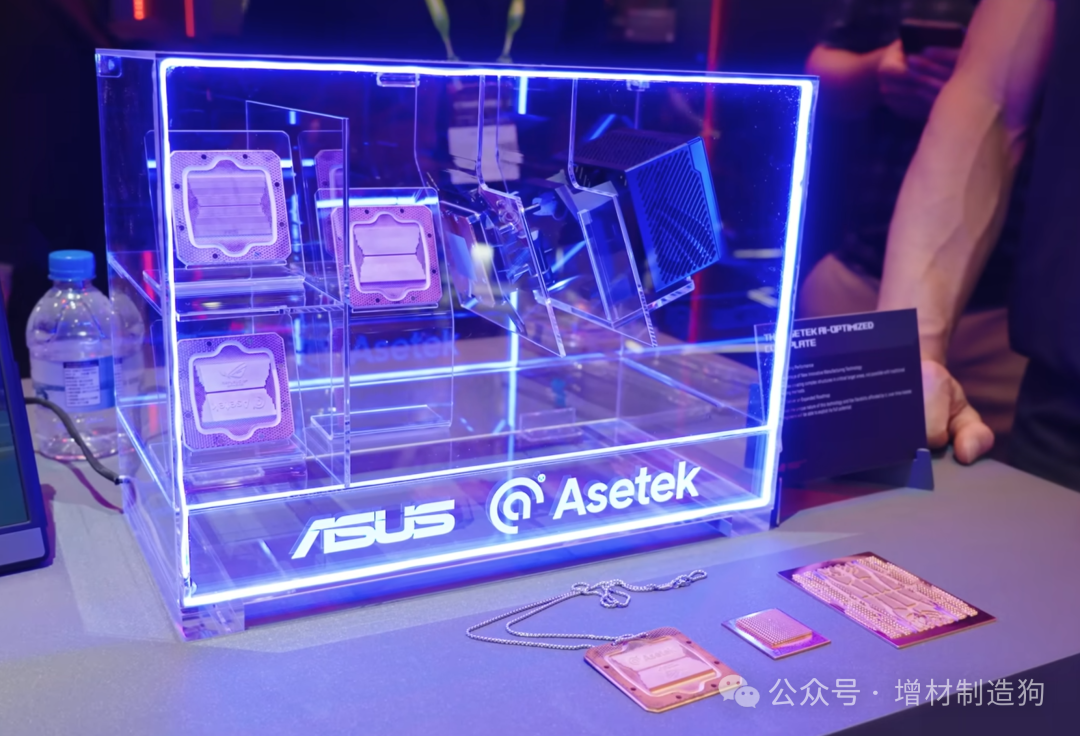
The story begins with a startup called Fabric8Labs, led by Intel Capital. This California-based company has successfully “grown” micro-structured heatsinks directly on chip surfaces using its unique ECAM (Electrochemical Additive Manufacturing) technology. The significance of this signal lies in its discoverer—Intel’s strategic investment arm, which serves as a clear industry barometer. Their bet on Fabric8Labs indicates that the entire industry must begin to embrace disruptive manufacturing technologies from outside the semiconductor field to break through the “physical wall” of power consumption and heat dissipation.
The disruptive nature of ECAM technology is reflected in its comprehensive superiority over existing manufacturing paradigms across three dimensions: process, materials, and design.
Process Advantage: “Cold” processing. The core advantage of ECAM lies in room temperature manufacturing. The entire process involves no thermal input or high-temperature melting, allowing direct printing on highly sensitive semiconductor chips without causing any thermal damage, which is the “ticket” to enter the semiconductor packaging field. Additionally, the absence of thermal stress means that the finished product will not warp or deform, and it possesses excellent surface smoothness, which is crucial for high-frequency RF and fluid applications.
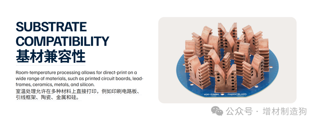
Material Advantage: “Pure” metals. ECAM can directly deposit over 99.9% pure metals (such as pure copper), rather than the alloy powders commonly used in other 3D printing technologies. The thermal and electrical conductivity of pure copper far exceeds that of alloys, making it the best choice for extreme heat dissipation and high-frequency electrical performance. The printed metal is a completely dense solid, comparable to forged metals.
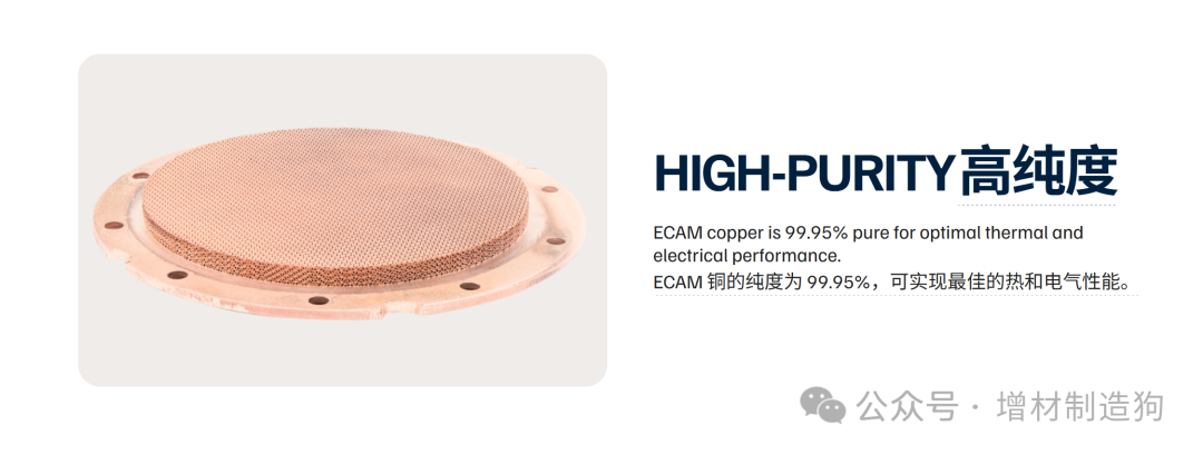
Design Advantage: “Integration.” It can “grow” functional structures on existing components, achieving true “integrated manufacturing,” eliminating performance bottlenecks caused by connection interfaces like thermal interface materials (TIM). At the same time, it perfectly adapts to AI-driven topological optimization designs, pushing product performance to theoretical limits.
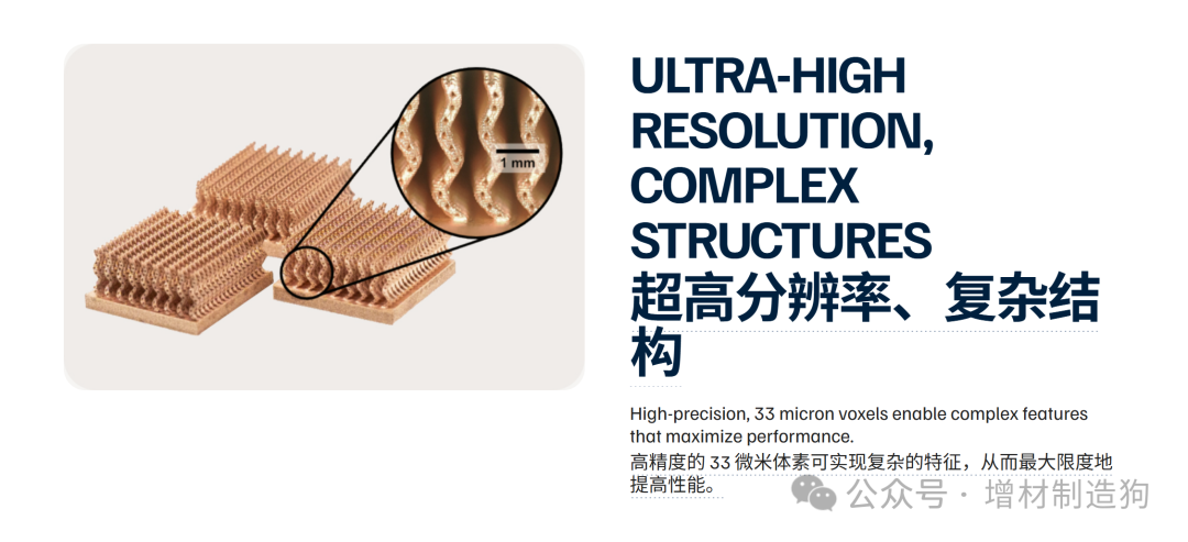
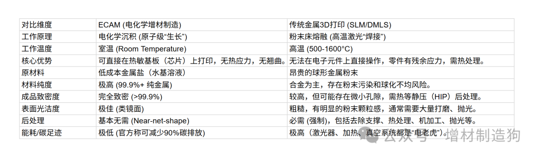 Through this comparison table, the commercial disruptive nature of ECAM is evident. It not only achieves breakthroughs inperformance (lossless printing, high purity, high precision) in new fields like semiconductors, but more importantly, it launches a “dimensionality reduction attack” oncost structure. The costs of traditional metal 3D printing are primarily driven by expensive equipment (lasers, vacuum chambers), costly raw materials (spherical powders), and complex post-processing procedures. ECAM fundamentally reshapes the cost curve by using inexpensive metal salts, low-power room temperature processes, and nearly zero post-processing requirements, paving the way for large-scale, low-cost commercial applications in the future.How ECAM Works Simply having good technology is not enough; Fabric8Labs’ true “moat” is a comprehensive system composed of multiple layers of barriers that are difficult to replicate.
Bottom Layer Barrier: The chemical black box of “process-materials.” Its core patent portfolio provides basic legal protection, while the specialized electrolyte formulations for different metals and applications are the real “secret sauce,” making it difficult for competitors to replicate.
Middle Layer Barrier: The intelligent control of “software-algorithms.” Converting 3D models into precise electric fields and current control requires extremely complex software and algorithms. This “design-manufacturing” closed-loop data flow, deeply integrated with AI-derived design tools, is its core competitive advantage.
Top Layer Barrier: Market access through “ecosystem-certification.” This is the highest and most solid commercial barrier. Entering the supply chain of semiconductor giants requires passing through extremely rigorous and lengthy certification processes. Once qualified as a supplier, a strong trust endorsement and market first-mover advantage are established, making it difficult for later entrants to shake.
Fabric8Labs Student Competition Promotion -2- Nano Dimension and the Macro Route of Additive Electronics (AME) -2- To understand the position of Fabric8Labs, we must introduce a reference point—the familiar additive electronics pioneer, Nano Dimension from Israel. Its core value lies in printing “development boards,” i.e., complete multilayer printed circuit boards (PCBs). By simultaneously jetting conductive silver ink and insulating polymer ink, Nano Dimension enables electronic engineers to turn complex circuit designs into reality within hours, greatly accelerating R&D iterations.
Nano Dimension
Dubin, WeChat Official Account: Additive Manufacturing Dog Express and Deep Dive | Nano Dimension Appoints New CEO, Insights into the Ambitions and Strategies of this “Electronic Printing” Unicorn
If Nano Dimension’s technology is like “building a complete highway system” (including insulated foundations and conductive lanes) on an empty lot, then Fabric8Labs’ technology is like “constructing a super interchange with extreme performance” at the most core and congested “traffic hub” of this highway. The former reshapes the macro process of electronic product R&D, while the latter aims to break through the micro performance bottlenecks of core components. This clearly reveals the evolution path of additive electronics: from the peripheral “circuit board level” to the core “chip level”; from optimizing the “system process” to breaking through the “core performance.”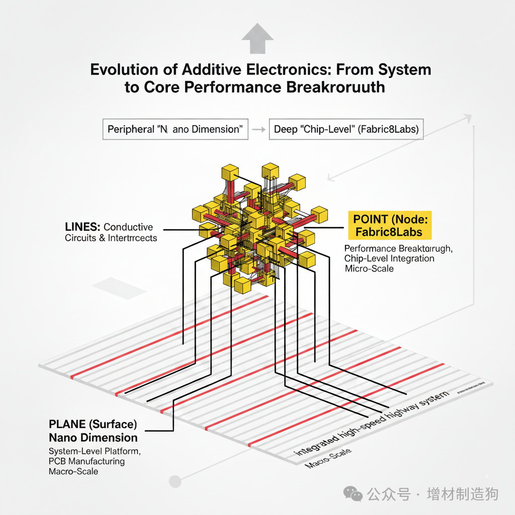 Both technical routes correspond to completely different commercial battlefields. Nano Dimension primarily targets the R&D departments of enterprises and fields such as military and aerospace that require small-batch, high-complexity customized circuits. Its core business model is “accelerating innovation, reducing costs, and increasing efficiency.” To build an ecosystem, it has integrated industry capabilities from AI software (DeepCube) to pick-and-place machines (Essemtec) through a series of strategic acquisitions, attempting to transform from a “printer manufacturer” to a “full-stack additive electronics solution provider,” but it also faces practical challenges in market promotion regarding costs, material systems, and customer education.
On the other hand, Fabric8Labs directly engages with semiconductor design companies (Fabless), IDMs, and packaging factories (OSAT). Its value lies in “unlocking performance and empowering design,” making chip designs that were previously impossible due to physical limitations feasible. The former optimizes processes in a saturated market, while the latter creates entirely new possibilities in an incremental market.
-3- The Flourishing of Micro-Manufacturing -3-
The field of additive electronics is not limited to the two companies mentioned above. There is another force also pushing the boundaries of micro-manufacturing, with different technological paths that together form a complete competitive landscape:
-
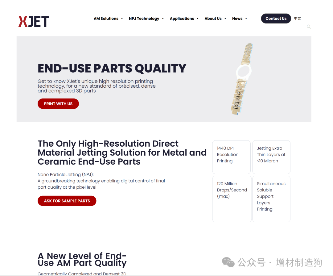
XJet (Israel): This is a strong competitor. Its uniqueNPJ (Nano Particle Jetting) technology manufactures solids by jetting “ink” containing metal or ceramic nanoparticles. It is also known for high precision and high-quality finished products, especially excelling in manufacturing small, precise metal and ceramic medical devices and electronic components.
https://xjet3d.com/
-
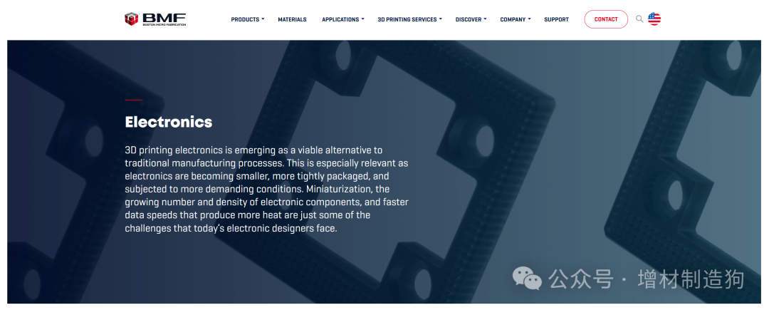
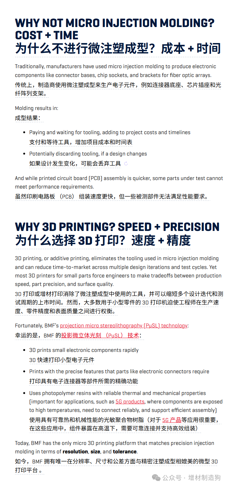
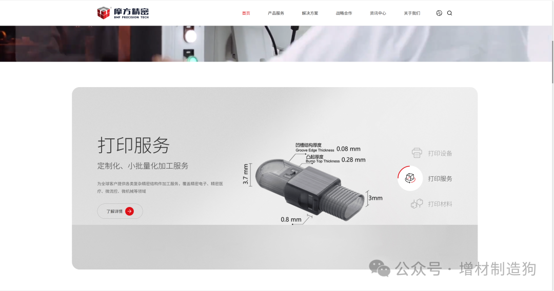
Boston Micro Fabrication (BMF, USA/China): BMF is a leader in the global micro 3D printing field, with itsPµSL (Projection Micro Stereolithography) technology achieving an astonishing 2-micron printing precision. Although its current main material is photosensitive resin, it has been widely applied in micro connectors, microfluidic chips, and micro-electromechanical systems (MEMS). It represents the trend of “making parts extremely small” and is an indispensable part of the entire additive electronics ecosystem.
https://bmf3d.com/3d-printing-electronics/
https://www.bmftec.cn/
-
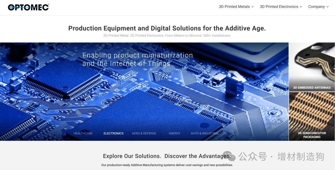
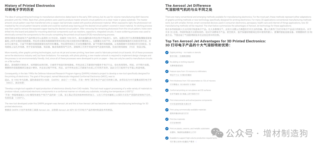
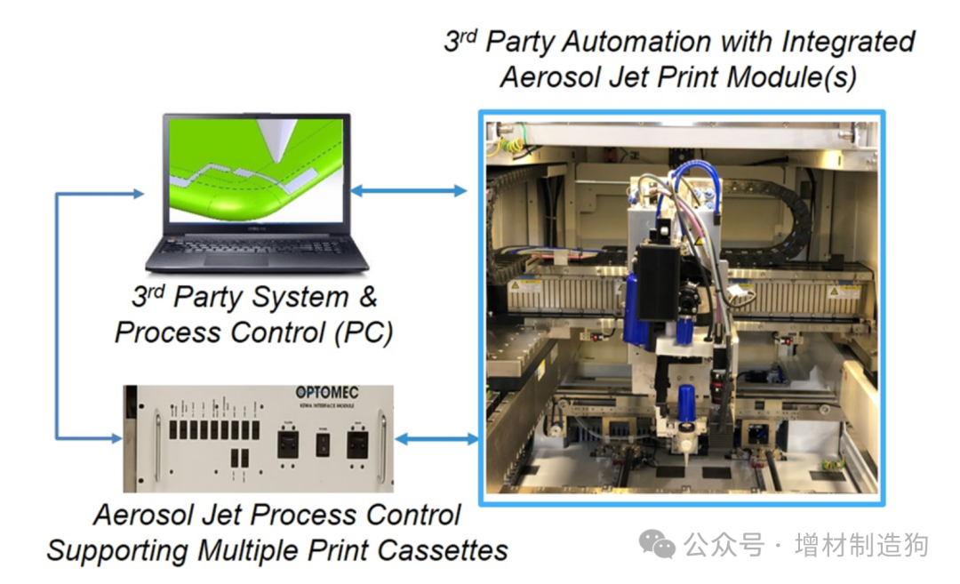
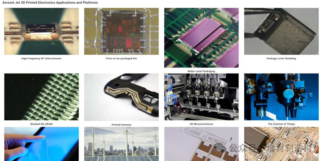
Optomec (USA): This is an established additive manufacturing company whoseAerosol Jet technology can print fine conductive lines, antennas, and sensors on complex three-dimensional surfaces. It focuses more on “adding” electronic functions to existing objects, such as printing antennas on the inner side of phone cases, making its applications very flexible.
https://optomec.com/printed-electronics/aerosol-jet-technology/
Currently, the entire additive electronics market is still in the “education phase” before an explosion, but the growth potential is enormous. These diverse technological paths are not entirely competitive but rather complementary, together forming the “toolbox” of micro-manufacturing. The future trend will be “multi-technology integration” and “deep binding of application scenarios.” No single technology can solve all problems; the future winners will undoubtedly be platform companies that can integrate various additive processes, materials, and AI design software to provide “end-to-end” solutions for specific industries (such as automotive radar, medical sensors, optical communication modules).
-4- Flagship Analysis · Chinese Perspective -4-
Having clearly depicted the global technological frontier, we can more objectively examine our own coordinates. The global additive electronics revolution presents both challenges and opportunities for China, which is committed to achieving industrial upgrades and technological independence. We must recognize that we are not lagging in all dimensions, but there are still significant gaps in the most critical areas.
China’s advantages and disadvantages present a stark “duality.”
-
Advantage: Strong system integration and market application capabilities. In the “system-level” cooling field, Chinese companies represented by Inspur and Alibaba have already taken the lead in the large-scale deployment of technologies like immersion liquid cooling. China has the largest and most active electronic product application market in the world, providing an unparalleled “testing ground” and “amplifier” for any new technology.
-
Disadvantage: Lack of core processes, materials, and equipment. In the “chip-level” micro-manufacturing domain, our industrial accumulation appears weak. Whether it is ECAM, NPJ, or PµSL, the core lies in the underlying precision equipment (such as high-precision nozzles, motion systems), key materials (such as specialized electrolytes, nano inks), and process control software. In these areas, we are still followers, with most research remaining at the laboratory stage.
For China, which is committed to achieving semiconductor independence, additive electronics undoubtedly offers a potential opportunity for a “leapfrog” approach. In traditional front-end equipment fields like photolithography machines and etching machines, we lag significantly behind the world’s top levels, and catching up will take a long time. However, in the emerging field of additive manufacturing, everyone is almost at the same starting line. If we can achieve breakthroughs in core processes and equipment like ECAM, we may bypass some of the “bottlenecked” traditional supply chains in the critical area of “advanced packaging” and establish unique, independent technological advantages. This is not only a technological catch-up but also a strategic game at the industrial level.
China’s breakthrough path should not be blind imitation but should leverage its unique advantage of “application-driven” innovation. Chinese entrepreneurs and investors should focus on finding “connection points” that can combine international cutting-edge technologies with China’s vast domestic demand. We should encourage more interdisciplinary innovation, supporting teams that understand material chemistry, software algorithms, and semiconductor processes. By continuously iterating, optimizing, and reducing costs in specific application scenarios (such as the three-electric system of new energy vehicles, and the irregular antennas of high-end consumer electronics), we have every opportunity to carve out our own rise from application to core in this “new electronic continent.” For capital, this requires “patience” that transcends short-term trends, as what is invested is not just capital but a possibility for the future of Chinese manufacturing.
Looking back at the entire text, a clear industry blueprint has unfolded: from the pioneering “printed circuit boards” initiated by Nano Dimension, to Fabric8Labs bringing the battlefield to the more core “chip packaging” level, and then to companies like XJet and BMF continuously enhancing the precision and material diversity of micro-manufacturing from different dimensions.
They collectively reveal a trend:3D printing is transitioning from “manufacturing forms” to “manufacturing functions”. As printing precision enters the micron level, and printing materials expand from plastics and metals to conductive, insulating, and dielectric materials, an era of “species explosion” belonging to additive electronics has arrived.
For those of us in the manufacturing industry, this is not just another new technology. It signifies that the rules of product design, supply chain logic, and even business models may be reshaped. This “new electronic continent” cultivated by additive technology deserves our continuous and in-depth attention.
About “Additive Manufacturing Dog” We are not a media outlet that only chases trends, but a solidly grounded, iteratively fast knowledge platform. We believe: “Information should be understandable and serve a purpose” Our identity is that of curiosity-driven explorers and systematic scholars. We do not provide standard answers but explore the forefront of the industry with you— the future decision-makers— together. Our mission: We select and decode those signals that can truly trigger industry changes from the global technological noise for you. We are committed to providing you with the highest quality “structured insights” to help you recognize the world with the highest efficiency and execute swiftly.<img src=”https://mmbiz.qpic.cn/mmbiz_png/zs1lfia1tiaJ7R1xbibpzsPNiaa4vLCTHrrssWBz9cpfR2ejmdIMia7meJ3icwEzV02cPGHVuia2IgFEnCJC5uPqjhIeA/640?wx_fmt=png&from=appmsg&watermark=1#imgIndex=16″