The direction of the board entering the wave soldering process should be indicated on the PCB, and the entry direction should be reasonable. If the PCB can enter from two directions, a double arrow entry indication should be used. (For reflow soldering, consider using tooling fixtures to determine the direction of passing through the reflow soldering.)
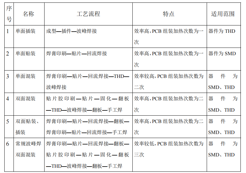
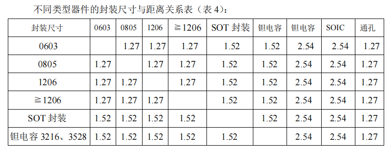
1. The safe distance for components on the back of the board that require wave soldering, which does not create a shadow effect, has considered the distance requirements for SMT components as follows:
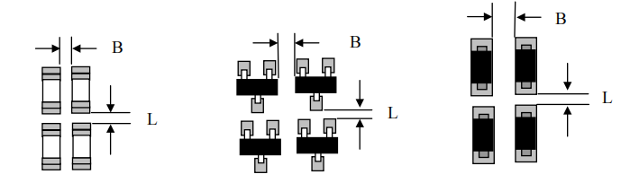
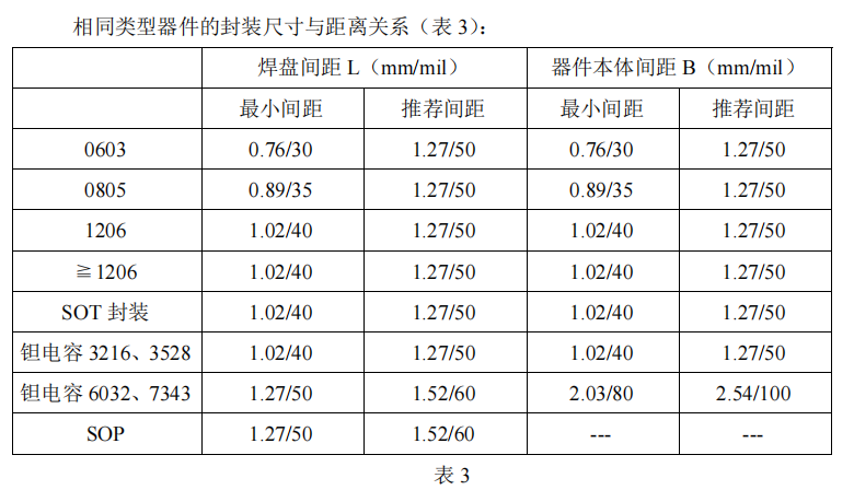
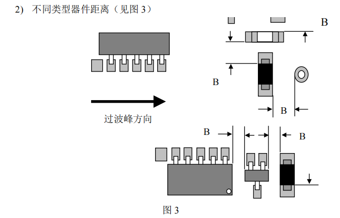
1) Distance between the same type of components (see Figure 2)

2. For ceramic capacitors larger than 0805, try to place them close to the transfer edge or in areas with less stress, and align their axis as parallel to the entry direction as possible (see Figure 4). Avoid using ceramic capacitors larger than 1825. (Reserved opinion)
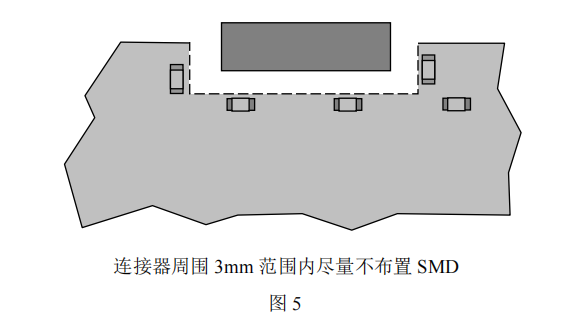
3. Avoid placing SMD components within a 3mm range around frequently inserted and removed devices or board edge connectors to prevent stress damage to components during connector insertion and removal. As shown in Figure 5:
The stand-off of surface-mounted devices passing through wave soldering meets the specification requirements.
The stand-off of surface-mounted devices passing through wave soldering should be less than 0.15mm; otherwise, they cannot be placed on the B-side for wave soldering. If the stand-off of the device is between 0.15mm and 0.2mm, copper foil can be placed under the device body to reduce the distance between the device body bottom and the PCB surface.
4. The minimum safe distance for back-side test points not to connect solder during wave soldering has been determined.
To ensure no solder connection during wave soldering, the distance between the edges of back-side test points should be greater than 1.0mm.
5. The pad spacing for plug-in components during wave soldering should be greater than 1.0mm.
To ensure no solder connection during wave soldering, the edge spacing of the pads for plug-in components should be greater than 1.0mm (including the edge spacing of the component pins).
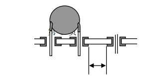
It is preferred that the pin pitch of plug-in components is ≧2.0mm, and the pad edge spacing is ≧1.0mm. Under the premise that the device bodies do not interfere with each other, the edge spacing of adjacent device pads should meet the requirements shown in the figure below:
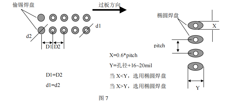
For plug-in components, the maximum number of pins per row should be arranged parallel to the entry direction of the pads. When the edge spacing of adjacent pads is 0.6mm–1.0mm, it is recommended to use oval pads or add solder pads (see Figure 7).
6. No components within 3mm of the BGA.
To ensure maintainability, a 3mm no-placement zone must be left around BGA components, with a preferred no-placement zone of 5mm. Generally, BGA components are not allowed to be placed on the back side (the board that has undergone reflow soldering twice, with the first side being the reflow soldering side); when there are BGA components on the back side, no components can be placed within the projection range of the 5mm no-placement zone on the front side BGA.
7. The minimum spacing between surface-mounted components meets the requirements.
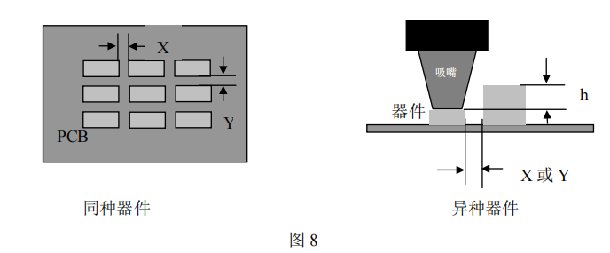
The distance requirements for machine-mounted components (see Figure 8):
Same type of components: ≧0.3mm
Different types of components: ≧0.13*h+0.3mm (h is the maximum height difference of surrounding neighboring components). The distance requirement for components that can only be manually placed is: ≧1.5mm.
8. The outer side of components should be greater than or equal to 5mm from the two edges of the board that contact the board track.
Technical Disclaimer:
If there are disputes over any indicators, labeling errors, or if further discussion is needed, we welcome technical feedback and corrections.