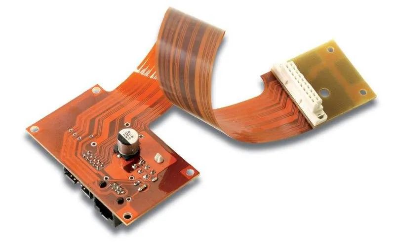
FPC, also known as flexible printed circuit board, has a significantly different PCBA assembly and soldering process compared to rigid circuit boards. Due to the insufficient hardness of the FPC boards, which are relatively soft, it is impossible to complete the basic SMT processes such as printing, mounting, and reflow without using a dedicated carrier board.
1. FPC Pre-treatment
The FPC boards are relatively soft and are generally not vacuum packed when they leave the factory. During transportation and storage, they easily absorb moisture from the air. Therefore, they need to undergo a pre-baking treatment before SMT placement to slowly force out the moisture. Otherwise, under the high-temperature impact of reflow soldering, the moisture absorbed by the FPC quickly vaporizes into steam, which can cause delamination, bubbling, and other defects.
The pre-baking conditions are generally a temperature of 80-100℃ for 4-8 hours. In special cases, the temperature can be raised to above 125℃, but the baking time must be correspondingly shortened. Before baking, a small sample test must be conducted to determine whether the FPC can withstand the set baking temperature. It is also advisable to consult the FPC manufacturer for suitable baking conditions. During baking, the stacking of FPCs should not be too much; 10-20 PNL is appropriate. Some FPC manufacturers will place a piece of paper between each PNL for isolation, and it must be confirmed that this isolation paper can withstand the set baking temperature. If not, it should be removed before baking. The baked FPC should show no significant discoloration, deformation, or warping, and it must pass an IPQC inspection before being put into production.
2. Production of Dedicated Carrier Boards
Based on the CAD file of the circuit board, the hole positioning data of the FPC is read to manufacture high-precision FPC positioning templates and dedicated carrier boards. The diameter of the positioning pins on the positioning template must match the positioning holes on the carrier board and the FPC. Many FPCs are not of the same thickness due to the need to protect certain circuits or design reasons; some areas are thicker while others need to be thinner, and some may have reinforcing metal plates. Therefore, the joint between the carrier board and the FPC must be processed, polished, and grooved according to the actual situation to ensure the FPC is flat during printing and mounting. The material requirements for the carrier board are that it should be lightweight, thin, high-strength, absorb less heat, and dissipate heat quickly, and it should have minimal warping after multiple thermal shocks. Common materials for carrier boards include synthetic stone, aluminum plates, silicone plates, and special high-temperature magnetized steel plates.
3. Production Process
Here, we will detail the key points of FPC SMT using a standard carrier board as an example. When using silicone plates or magnetic fixtures, fixing the FPC is much easier, and tape is not required. The key points of the processes such as printing, mounting, and soldering remain the same.
Fixing the FPC
Before SMT, the FPC must be accurately fixed to the carrier board. It is particularly important that the storage time between fixing the FPC to the carrier board and performing printing, mounting, and soldering is as short as possible. There are two types of carrier boards: with positioning pins and without positioning pins. Carrier boards without positioning pins must be used in conjunction with positioning templates that have pins. First, the carrier board is placed over the positioning pins of the template, allowing the pins to pass through the positioning holes on the carrier board. Then, each FPC is placed over the exposed positioning pins and secured with tape. After this, the carrier board is separated from the FPC positioning template for printing, mounting, and soldering. Carrier boards with positioning pins already have several spring positioning pins fixed, allowing each FPC to be directly placed onto the spring pins and then secured with tape. In the printing process, the spring positioning pins can be completely pressed into the carrier board by the stencil, ensuring no impact on the printing quality.
Method 1 (Single-sided tape fixing): Use thin, high-temperature resistant single-sided tape to secure the four edges of the FPC to the carrier board, preventing any shifting or warping. The tape’s adhesion should be moderate, allowing for easy peeling after reflow soldering, with no residual adhesive left on the FPC. If using an automatic tape dispenser, it can quickly cut uniform lengths of tape, significantly improving efficiency, saving costs, and avoiding waste.
Method 2 (Double-sided tape fixing): First, apply high-temperature resistant double-sided tape to the carrier board, achieving the same effect as using a silicone board, and then adhere the FPC to the carrier board. Special attention should be paid to ensure the tape’s adhesion is not too high; otherwise, during peeling after reflow soldering, it can easily cause the FPC to tear. After multiple passes through the oven, the adhesion of the double-sided tape will gradually decrease, and when it becomes insufficient to reliably secure the FPC, it must be replaced immediately. This workstation is critical for preventing FPC contamination and requires the use of finger cots during operation. Before reusing the carrier board, it must be properly cleaned, which can be done with a non-woven cloth soaked in cleaning agents or with an anti-static dust removal roller to remove surface dust, solder balls, and other foreign materials. When handling the FPC, avoid applying too much force, as the FPC is fragile and can easily crease or break.
FPC Solder Paste Printing
FPC does not have very specific requirements for solder paste composition; the size of solder balls and metal content depend on whether there are fine-pitch ICs on the FPC. However, FPC has high requirements for solder paste printing performance. The solder paste should have excellent thixotropy, allowing it to be easily printed and released, and it should firmly adhere to the FPC surface without poor release, clogging the stencil openings, or collapsing after printing.
Since the FPC is mounted on the carrier board, and there are high-temperature resistant tapes for positioning, the surfaces cannot be as flat as those of PCBs, and there will definitely be local gaps between the FPC and the carrier board. Therefore, the drop height of the nozzle, air pressure, etc., must be precisely set, and the nozzle movement speed must be reduced. Additionally, since FPCs are often in panels, and the yield rate of FPCs is relatively low, it is common for the entire PNL to contain some defective pieces. Thus, the placement machine must be equipped with BAD MARK recognition functionality; otherwise, production efficiency will be significantly affected when producing such non-uniform panels.
FPC Reflow Soldering
A forced hot air convection infrared reflow soldering oven should be used, as this allows for a more uniform temperature change on the FPC, reducing the occurrence of soldering defects. If single-sided tape is used, since it can only secure the four edges of the FPC, the middle part may deform under hot air conditions, causing the pads to tilt, and molten solder (liquid solder at high temperatures) may flow, leading to cold solder joints, bridging, and solder balls, resulting in a higher defect rate.
1) Temperature Curve Testing Method
Due to the different heat absorption characteristics of the carrier board and the different types of components on the FPC, the rate of temperature rise during reflow soldering varies, and the amount of heat absorbed also differs. Therefore, carefully setting the temperature curve of the reflow soldering oven greatly impacts soldering quality. A more reliable method is to place two carrier boards with FPCs on both sides of the test board during actual production, with components mounted on the FPC of the test board. Use high-temperature solder wire to solder temperature probe tips to the test points and secure the probe leads to the carrier board with high-temperature tape, ensuring that the tape does not cover the test points. The test points should be chosen near the edges of the carrier board and at solder joints and QFP pins; such test results will better reflect the actual situation.
2) Setting the Temperature Curve
During oven temperature debugging, because FPCs do not have good thermal uniformity, it is best to use a temperature curve approach of heating/holding/flowing, making it easier to control the parameters in each temperature zone. Additionally, the thermal shock impact on the FPC and components will be smaller. Based on experience, it is advisable to set the oven temperature to the lower limit of the solder paste technical requirements, and the wind speed in the reflow oven should generally be set to the lowest speed that the oven can achieve, ensuring the stability of the reflow oven chain without any shaking.
FPC Inspection, Testing, and Panel Separation
Since the carrier board absorbs heat during the oven process, especially aluminum carrier boards, the temperature is relatively high upon exiting the oven. Therefore, it is best to add forced cooling fans at the exit to help cool down quickly. At the same time, operators should wear heat-resistant gloves to avoid burns from the hot carrier boards. When taking the completed FPC off the carrier board, the force must be even; do not use excessive force to avoid tearing or creasing the FPC.
The removed FPC should be visually inspected under a magnifying glass with at least 5x magnification, focusing on checking for residual adhesive, discoloration, solder on gold fingers, solder balls, cold solder joints, bridging, and other issues. Due to the uneven surface of the FPC, the false detection rate of AOI is very high, so FPCs are generally not suitable for AOI inspection. However, with the help of special testing fixtures, FPCs can complete ICT and FCT testing.
Since FPCs are mostly in panels, it may be necessary to perform panel separation before conducting ICT and FCT testing. Although knives, scissors, and other tools can be used for panel separation, the efficiency and quality of the operation are low, leading to a high scrap rate. For large-scale production of irregular FPCs, it is recommended to make dedicated FPC stamping separation molds for punching, which can significantly improve operational efficiency. Additionally, the edges of the stamped FPC will be neat and aesthetically pleasing, and the internal stress generated during stamping will be very low, effectively avoiding solder joint cracking.
In the assembly and soldering process of PCBA flexible electronics, the precise positioning and fixing of FPCs are key. The critical factor for good fixation is the production of suitable carrier boards. Next are the pre-baking of FPCs, printing, mounting, and reflow soldering. It is clear that the SMT process for FPCs is significantly more challenging than for PCB rigid boards, so precise setting of process parameters is necessary. Additionally, strict production process management is equally important, ensuring that operators strictly follow every regulation in the SOP, and that line engineers and IPQC strengthen inspections to promptly identify abnormalities in the production line, analyze the causes, and take necessary measures to control the defect rate of the FPC SMT production line to within dozens of PPM.
In the PCBA production process, many machines and equipment are required to assemble a board, and often the quality level of a factory’s machinery directly determines its manufacturing capability.
The basic equipment required for PCBA production includes solder paste printers, placement machines, reflow ovens, AOI testers, component lead cutting machines, wave soldering machines, solder furnaces, board washing machines, ICT testing fixtures, FCT testing fixtures, and aging test racks. The equipment equipped will vary in different scales of PCBA processing plants.
4. PCBA Production Equipment
Solder Paste Printer
Modern solder paste printers typically consist of components for board loading, solder paste application, printing, and circuit board transfer. Its working principle is as follows: first, the circuit board to be printed is fixed on the printing positioning table, and then the left and right blades of the printer apply solder paste or red glue through a stencil onto the corresponding pads. The uniformly printed PCBs are then transferred to the placement machine for automatic placement.
2
Placement Machine
The placement machine, also known as the “pick-and-place machine” or “Surface Mount System,” is positioned after the solder paste printer on the production line. It accurately places surface-mounted components onto the PCB pads using a moving placement head. It can be manual or fully automatic.
3
Reflow Soldering
The reflow soldering machine has a heating circuit that blows heated air or nitrogen at a sufficiently high temperature onto the circuit board that has components mounted, causing the solder on both sides of the components to melt and bond with the main board. The advantages of this process include easy temperature control, avoiding oxidation during soldering, and easier control of manufacturing costs.
4
AOI Tester
AOI stands for Automatic Optical Inspection, a device that detects common defects encountered during the soldering process based on optical principles. AOI is a new testing technology that has developed rapidly, with many manufacturers releasing AOI testing equipment. During automatic inspection, the machine automatically scans the PCB with a camera, collects images, compares the solder joints being tested with qualified parameters in a database, and through image processing, identifies defects on the PCB, displaying/marking the defects on a monitor or automatically.
5
Component Lead Cutting Machine
This is used for cutting and deforming the leads of through-hole components.
6
Wave Soldering
Wave soldering involves direct contact of the soldering surface of the plug-in board with high-temperature liquid solder to achieve soldering, where the high-temperature liquid solder maintains an inclined surface and forms wave-like phenomena through special devices, hence the name “wave soldering.” The main material used is solder bars.
7
Solder Furnace
Generally, a solder furnace refers to a welding tool used in electronics soldering. It provides good consistency in soldering for discrete component circuit boards, is easy to operate, quick, and highly efficient, making it a good helper for your production processing.
8
Board Washing Machine
This is used for cleaning PCBA boards, effectively removing residues after soldering.
9
ICT Testing Fixture
ICT testing mainly involves testing probes contacting the test points on the PCB layout to detect open circuits, short circuits, and the soldering status of all components on the PCBA.
10
FCT Testing Fixture
FCT (Functional Testing) refers to providing a simulated operating environment (stimulus and load) for the test target board (UUT: Unit Under Test), allowing it to operate under various design states to obtain parameters for verifying the functionality of the UUT. In simple terms, it involves applying appropriate stimuli to the UUT and measuring whether the output response meets requirements.
11
Aging Test Rack
The aging test rack can conduct batch testing on PCBA boards, simulating user operations over extended periods to identify problematic PCBA boards.
PCBA outsourcing refers to PCBA processing manufacturers outsourcing PCBA orders to other capable PCBA processing manufacturers. What requirements are generally involved in PCBA outsourcing?
Bill of Materials
Components should be inserted or mounted according to the bill of materials, PCB silk screen, and outsourcing processing requirements. If there are discrepancies between the materials and the bill, PCB silk screen, or if there are contradictions or ambiguities in the process requirements that prevent operation, please contact our company promptly to confirm the correctness of the materials and process requirements.
Anti-static Requirements
1. All components should be treated as electrostatic sensitive devices.
2. All personnel who come into contact with components and products should wear anti-static clothing, anti-static wristbands, and anti-static shoes.
3. During the raw material entry and warehousing phase, electrostatic sensitive devices should be packaged in anti-static materials.
4. During operations, use anti-static work surfaces, and store components and semi-finished products in anti-static containers.
5. Soldering equipment must be reliably grounded, and electric soldering irons should be anti-static types, tested before use.
6. Semi-finished PCB storage and transportation should use anti-static boxes, with anti-static pearl cotton for isolation.
7. For unencased machines, use anti-static packaging bags.
Regulations on Component Appearance Marking and Insertion Direction
1. Polarized components should be inserted according to polarity.
2. For components with silk screen on the side (e.g., high-voltage ceramic capacitors), when inserted vertically, the silk screen should face right; when inserted horizontally, the silk screen should face down. For components with silk screen on the top (excluding surface mount resistors), when inserted horizontally, the text direction should match the silk screen direction on the PCB; when inserted vertically, the top of the text should face right.
3. For resistors inserted horizontally, the error color ring should face right; when inserted vertically, the error color ring should face down; when inserted upright, the error color ring should face the board surface.
Soldering Requirements
1. The height of the leads of inserted components should be 1.5-2.0mm above the soldering surface. Surface-mounted components should lie flat against the board surface, with solder joints smooth and without burrs, slightly arched, and the solder should exceed 2/3 of the lead height but should not exceed the lead height. Insufficient solder or solder joints appearing as balls or covering the surface mount are considered defects;
2. Solder joint height: The solder should climb the lead height on single-sided boards by no less than 1mm, and on double-sided boards by no less than 0.5mm, and must be visible through the solder.
3. Solder joint shape: Should be conical and cover the entire pad.
4. Solder joint surface: Smooth and bright, without black spots, flux residues, or other debris, and without spurs, pits, air holes, or exposed copper defects.
5. Solder joint strength: Should be adequately wetted to the pad and lead, with no cold solder or false solder.
6. Solder joint cross-section: Component leads should ideally not be cut into the solder area, with no cracks in the solder at the contact surface between leads and solder. No spurs or barbs should be present at the cross-section.
7. Socket soldering: The socket should be inserted with the bottom against the board, and the position should be correct. After soldering the socket, the bottom should not float more than 0.5mm, and the body should not be skewed beyond the silk screen frame. Rows of sockets should also be kept neat, with no front-back misalignment or uneven heights.
Transportation
To prevent damage to PCBA during transportation, the following packaging should be used:
1. Container: Anti-static turnover boxes.
2. Isolation material: Anti-static pearl cotton.
3. Placement spacing: There should be more than 10mm distance between PCBs and between PCBs and the container.
4. Placement height: There should be more than 50mm space from the top of the turnover box to ensure that the turnover box does not press down on the power supply, especially for wired power supplies.
Washing Requirements and Others
The board surface should be clean, free of solder balls, component leads, and stains. Particularly, there should be no soldering residues visible at the solder joints on the plug-in side. During washing, the following components should be protected: wires, connection terminals, relays, switches, polyester capacitors, and other easily corroded components. It is strictly forbidden to use ultrasonic cleaning on relays.
All components must be installed within the edges of the PCB.
During the PCBA oven process, due to the washing of the leads of plug-in components by solder flow, some plug-in components may be tilted after soldering, causing the component body to extend beyond the silk screen frame. Therefore, soldering personnel after the solder furnace should make appropriate corrections.